RCV56HCF PCI/CardBus Modem Designer’s Guide
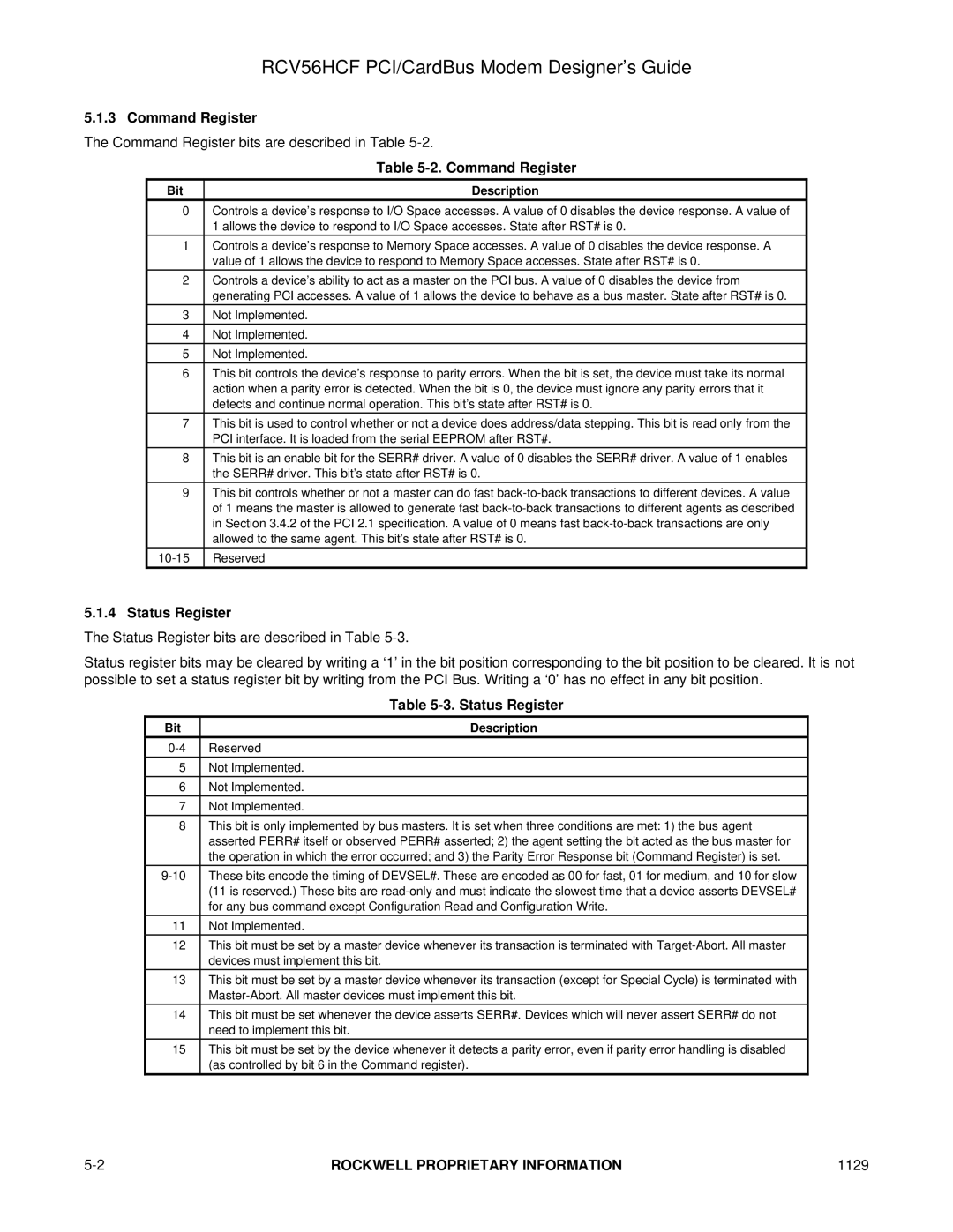
5.1.3 Command Register
The Command Register bits are described in Table
| Table |
Bit | Description |
0 | Controls a device’s response to I/O Space accesses. A value of 0 disables the device response. A value of |
| 1 allows the device to respond to I/O Space accesses. State after RST# is 0. |
1 | Controls a device’s response to Memory Space accesses. A value of 0 disables the device response. A |
| value of 1 allows the device to respond to Memory Space accesses. State after RST# is 0. |
2 | Controls a device’s ability to act as a master on the PCI bus. A value of 0 disables the device from |
| generating PCI accesses. A value of 1 allows the device to behave as a bus master. State after RST# is 0. |
|
|
3 | Not Implemented. |
4 | Not Implemented. |
5 | Not Implemented. |
|
|
6 | This bit controls the device’s response to parity errors. When the bit is set, the device must take its normal |
| action when a parity error is detected. When the bit is 0, the device must ignore any parity errors that it |
| detects and continue normal operation. This bit’s state after RST# is 0. |
7 | This bit is used to control whether or not a device does address/data stepping. This bit is read only from the |
| PCI interface. It is loaded from the serial EEPROM after RST#. |
8 | This bit is an enable bit for the SERR# driver. A value of 0 disables the SERR# driver. A value of 1 enables |
| the SERR# driver. This bit’s state after RST# is 0. |
9 | This bit controls whether or not a master can do fast |
| of 1 means the master is allowed to generate fast |
| in Section 3.4.2 of the PCI 2.1 specification. A value of 0 means fast |
| allowed to the same agent. This bit’s state after RST# is 0. |
Reserved | |
|
|
5.1.4 Status Register
The Status Register bits are described in Table
Status register bits may be cleared by writing a ‘1’ in the bit position corresponding to the bit position to be cleared. It isnot possible to set a status register bit by writing from the PCI Bus. Writing a ‘0’ has no effect in any bit position.
| Table |
Bit | Description |
Reserved | |
|
|
5 | Not Implemented. |
6 | Not Implemented. |
|
|
7 | Not Implemented. |
8 | This bit is only implemented by bus masters. It is set when three conditions are met: 1) the bus agent |
| asserted PERR# itself or observed PERR# asserted; 2) the agent setting the bit acted as the bus master for |
| the operation in which the error occurred; and 3) the Parity Error Response bit (Command Register) is set. |
These bits encode the timing of DEVSEL#. These are encoded as 00 for fast, 01 for medium, and 10 for slow | |
| (11 is reserved.) These bits are |
| for any bus command except Configuration Read and Configuration Write. |
11 | Not Implemented. |
|
|
12 | This bit must be set by a master device whenever its transaction is terminated with |
| devices must implement this bit. |
|
|
13 | This bit must be set by a master device whenever its transaction (except for Special Cycle) is terminated with |
| |
14 | This bit must be set whenever the device asserts SERR#. Devices which will never assert SERR# do not |
| need to implement this bit. |
15 | This bit must be set by the device whenever it detects a parity error, even if parity error handling is disabled |
| (as controlled by bit 6 in the Command register). |
ROCKWELL PROPRIETARY INFORMATION | 1129 |