|
| RCV56HCF PCI/CardBus Modem Designer’s Guide | |
|
|
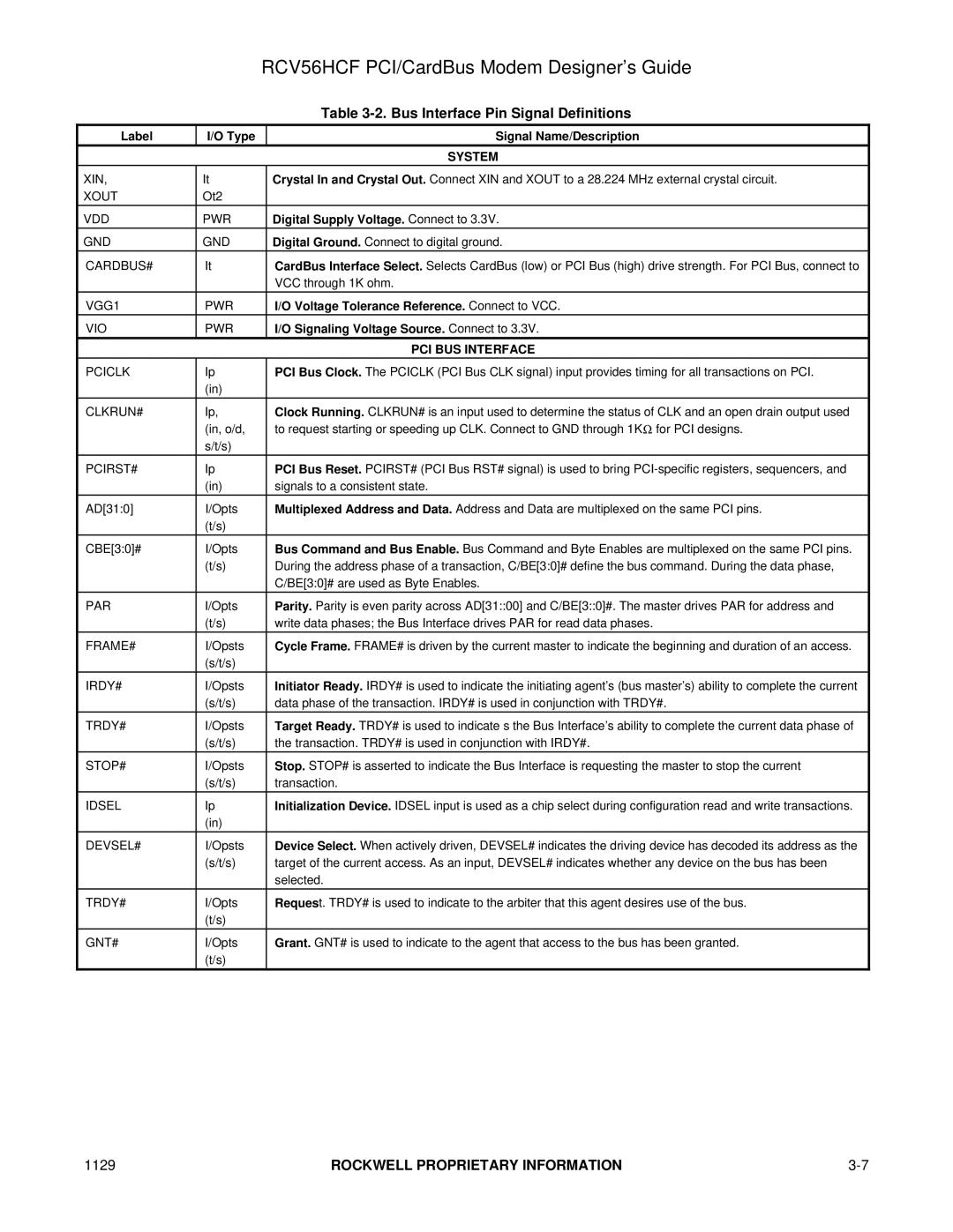
| Table |
|
|
|
|
Label | I/O Type |
| Signal Name/Description |
|
|
| SYSTEM |
XIN, | It |
| Crystal In and Crystal Out. Connect XIN and XOUT to a 28.224 MHz external crystal circuit. |
XOUT | Ot2 |
|
|
|
|
|
|
VDD | PWR |
| Digital Supply Voltage. Connect to 3.3V. |
GND | GND |
| Digital Ground. Connect to digital ground. |
CARDBUS# | It |
| CardBus Interface Select. Selects CardBus (low) or PCI Bus (high) drive strength. For PCI Bus, connect to |
|
|
| VCC through 1K ohm. |
|
|
|
|
VGG1 | PWR |
| I/O Voltage Tolerance Reference. Connect to VCC. |
VIO | PWR |
| I/O Signaling Voltage Source. Connect to 3.3V. |
|
|
| PCI BUS INTERFACE |
PCICLK | Ip |
| PCI Bus Clock. The PCICLK (PCI Bus CLK signal) input provides timing for all transactions on PCI. |
| (in) |
|
|
|
|
|
|
CLKRUN# | Ip, |
| Clock Running. CLKRUN# is an input used to determine the status of CLK and an open drain output used |
| (in, o/d, |
| to request starting or speeding up CLK. Connect to GND through 1KΩ for PCI designs. |
| s/t/s) |
|
|
|
|
|
|
PCIRST# | Ip |
| PCI Bus Reset. PCIRST# (PCI Bus RST# signal) is used to bring |
| (in) |
| signals to a consistent state. |
AD[31:0] | I/Opts |
| Multiplexed Address and Data. Address and Data are multiplexed on the same PCI pins. |
| (t/s) |
|
|
CBE[3:0]# | I/Opts |
| Bus Command and Bus Enable. Bus Command and Byte Enables are multiplexed on the same PCI pins. |
| (t/s) |
| During the address phase of a transaction, C/BE[3:0]# define the bus command. During the data phase, |
|
|
| C/BE[3:0]# are used as Byte Enables. |
PAR | I/Opts |
| Parity. Parity is even parity across AD[31::00] and C/BE[3::0]#. The master drives PAR for address and |
| (t/s) |
| write data phases; the Bus Interface drives PAR for read data phases. |
FRAME# | I/Opsts |
| Cycle Frame. FRAME# is driven by the current master to indicate the beginning and duration of an access. |
| (s/t/s) |
|
|
|
|
|
|
IRDY# | I/Opsts |
| Initiator Ready. IRDY# is used to indicate the initiating agent’s (bus master’s) ability to complete the current |
| (s/t/s) |
| data phase of the transaction. IRDY# is used in conjunction with TRDY#. |
|
|
|
|
TRDY# | I/Opsts |
| Target Ready. TRDY# is used to indicate s the Bus Interface’s ability to complete the current data phase of |
| (s/t/s) |
| the transaction. TRDY# is used in conjunction with IRDY#. |
STOP# | I/Opsts |
| Stop. STOP# is asserted to indicate the Bus Interface is requesting the master to stop the current |
| (s/t/s) |
| transaction. |
IDSEL | Ip |
| Initialization Device. IDSEL input is used as a chip select during configuration read and write transactions. |
| (in) |
|
|
|
|
|
|
DEVSEL# | I/Opsts |
| Device Select. When actively driven, DEVSEL# indicates the driving device has decoded its address as the |
| (s/t/s) |
| target of the current access. As an input, DEVSEL# indicates whether any device on the bus has been |
|
|
| selected. |
TRDY# | I/Opts |
| Request. TRDY# is used to indicate to the arbiter that this agent desires use of the bus. |
| (t/s) |
|
|
|
|
|
|
GNT# | I/Opts |
| Grant. GNT# is used to indicate to the agent that access to the bus has been granted. |
| (t/s) |
|
|
1129 | ROCKWELL PROPRIETARY INFORMATION |