Intel® PXA27x Processor Family Power Requirements
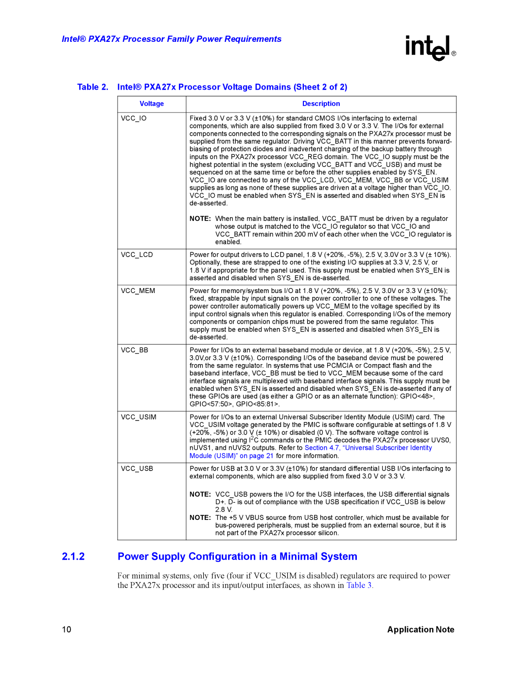
Table 2. Intel® PXA27x Processor Voltage Domains (Sheet 2 of 2)
Voltage | Description |
|
|
VCC_IO | Fixed 3.0 V or 3.3 V (±10%) for standard CMOS I/Os interfacing to external |
| components, which are also supplied from fixed 3.0 V or 3.3 V. The I/Os for external |
| components connected to the corresponding signals on the PXA27x processor must be |
| supplied from the same regulator. Driving VCC_BATT in this manner prevents forward- |
| biasing of protection diodes and inadvertent charging of the backup battery through |
| inputs on the PXA27x processor VCC_REG domain. The VCC_IO supply must be the |
| highest potential in the system (excluding VCC_BATT and VCC_USB) and must be |
| sequenced on at the same time or before the other supplies enabled by SYS_EN. |
| VCC_IO are connected to any of the VCC_LCD, VCC_MEM, VCC_BB or VCC_USIM |
| supplies as long as none of these supplies are driven at a voltage higher than VCC_IO. |
| VCC_IO must be enabled when SYS_EN is asserted and disabled when SYS_EN is |
| |
| NOTE: When the main battery is installed, VCC_BATT must be driven by a regulator |
| whose output is matched to the VCC_IO regulator so that VCC_IO and |
| VCC_BATT remain within 200 mV of each other when the VCC_IO regulator is |
| enabled. |
|
|
VCC_LCD | Power for output drivers to LCD panel, 1.8 V (+20%, |
| Optionally, these are strapped to one of the existing I/O supplies at 3.3 V, 2.5 V, or |
| 1.8 V if appropriate for the panel used. This supply must be enabled when SYS_EN is |
| asserted and disabled when SYS_EN is |
|
|
VCC_MEM | Power for memory/system bus I/O at 1.8 V (+20%, |
| fixed, strappable by input signals on the power controller to one of these voltages. The |
| power controller automatically powers up VCC_MEM to the voltage specified by its |
| input control signals when this regulator is enabled. Corresponding I/Os of the memory |
| components or companion chips must be powered from the same regulator. This |
| supply must be enabled when SYS_EN is asserted and disabled when SYS_EN is |
| |
|
|
VCC_BB | Power for I/Os to an external baseband module or device, at 1.8 V (+20%, |
| 3.0V,or 3.3 V (±10%). Corresponding I/Os of the baseband device must be powered |
| from the same regulator. In systems that use PCMCIA or Compact flash and the |
| baseband interface, VCC_BB must be tied to VCC_MEM because some of the card |
| interface signals are multiplexed with baseband interface signals. This supply must be |
| enabled when SYS_EN is asserted and disabled when SYS_EN is |
| these GPIOs are used (as either a GPIO or as an alternate function): GPIO<48>, |
| GPIO<57:50>, GPIO<85:81>. |
|
|
VCC_USIM | Power for I/Os to an external Universal Subscriber Identity Module (USIM) card. The |
| VCC_USIM voltage generated by the PMIC is software configurable at settings of 1.8 V |
| (+20%, |
| implemented using I2C commands or the PMIC decodes the PXA27x processor UVS0, |
| nUVS1, and nUVS2 outputs. Refer to Section 4.7, “Universal Subscriber Identity |
| Module (USIM)” on page 21 for more information. |
|
|
VCC_USB | Power for USB at 3.0 V or 3.3V (±10%) for standard differential USB I/Os interfacing to |
| external components, which are also supplied from fixed 3.0 V or 3.3 V. |
| NOTE: VCC_USB powers the I/O for the USB interfaces, the USB differential signals |
| D+. D- is out of compliance with the USB specification if VCC_USB is below |
| 2.8 V. |
| NOTE: The +5 V VBUS source from USB host controller, which must be available for |
| |
| not part of the PXA27x processor silicon. |
|
|
2.1.2Power Supply Configuration in a Minimal System
For minimal systems, only five (four if VCC_USIM is disabled) regulators are required to power the PXA27x processor and its input/output interfaces, as shown in Table 3.
10 | Application Note |