Intel® PXA27x Processor Family Power Requirements
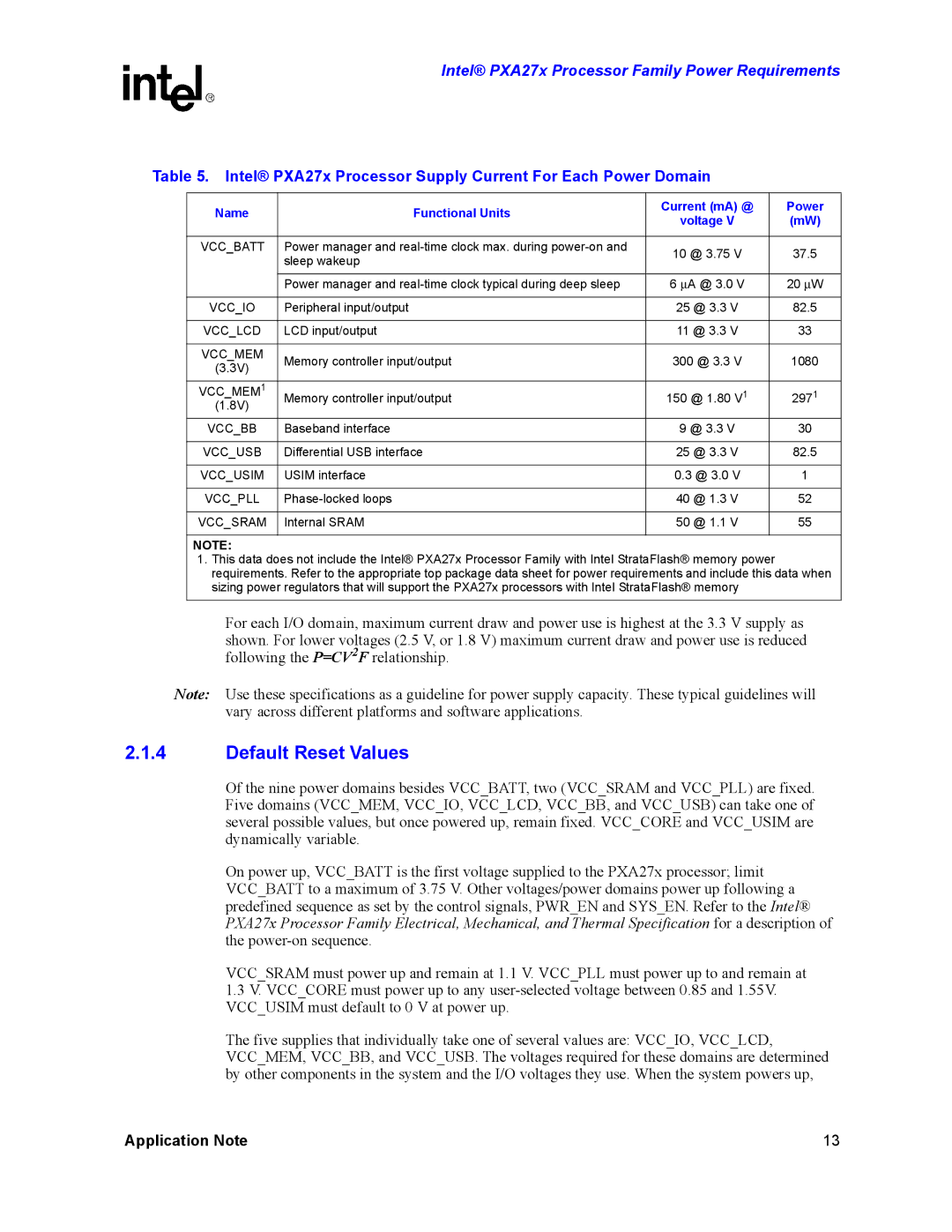
Table 5. Intel® PXA27x Processor Supply Current For Each Power Domain
Name | Functional Units | Current (mA) @ | Power | |
voltage V | (mW) | |||
|
| |||
|
|
|
| |
VCC_BATT | Power manager and | 10 @ 3.75 V | 37.5 | |
| sleep wakeup | |||
|
|
| ||
|
|
|
| |
| Power manager and | 6 ∝A @ 3.0 V | 20 ∝W | |
|
|
|
| |
VCC_IO | Peripheral input/output | 25 @ 3.3 V | 82.5 | |
|
|
|
| |
VCC_LCD | LCD input/output | 11 @ 3.3 V | 33 | |
|
|
|
| |
VCC_MEM | Memory controller input/output | 300 @ 3.3 V | 1080 | |
(3.3V) | ||||
|
|
| ||
|
|
|
| |
VCC_MEM1 | Memory controller input/output | 150 @ 1.80 V1 | 2971 | |
(1.8V) |
|
|
| |
VCC_BB | Baseband interface | 9 @ 3.3 V | 30 | |
|
|
|
| |
VCC_USB | Differential USB interface | 25 @ 3.3 V | 82.5 | |
|
|
|
| |
VCC_USIM | USIM interface | 0.3 @ 3.0 V | 1 | |
|
|
|
| |
VCC_PLL | 40 @ 1.3 V | 52 | ||
|
|
|
| |
VCC_SRAM | Internal SRAM | 50 @ 1.1 V | 55 | |
|
|
|
|
NOTE:
1. This data does not include the Intel® PXA27x Processor Family with Intel StrataFlash® memory power requirements. Refer to the appropriate top package data sheet for power requirements and include this data when sizing power regulators that will support the PXA27x processors with Intel StrataFlash® memory
For each I/O domain, maximum current draw and power use is highest at the 3.3 V supply as shown. For lower voltages (2.5 V, or 1.8 V) maximum current draw and power use is reduced following the P=CV2F relationship.
Note: Use these specifications as a guideline for power supply capacity. These typical guidelines will vary across different platforms and software applications.
2.1.4Default Reset Values
Of the nine power domains besides VCC_BATT, two (VCC_SRAM and VCC_PLL) are fixed. Five domains (VCC_MEM, VCC_IO, VCC_LCD, VCC_BB, and VCC_USB) can take one of several possible values, but once powered up, remain fixed. VCC_CORE and VCC_USIM are dynamically variable.
On power up, VCC_BATT is the first voltage supplied to the PXA27x processor; limit VCC_BATT to a maximum of 3.75 V. Other voltages/power domains power up following a predefined sequence as set by the control signals, PWR_EN and SYS_EN. Refer to the Intel® PXA27x Processor Family Electrical, Mechanical, and Thermal Specification for a description of the
VCC_SRAM must power up and remain at 1.1 V. VCC_PLL must power up to and remain at
1.3V. VCC_CORE must power up to any
The five supplies that individually take one of several values are: VCC_IO, VCC_LCD,
VCC_MEM, VCC_BB, and VCC_USB. The voltages required for these domains are determined by other components in the system and the I/O voltages they use. When the system powers up,
Application Note | 13 |