|
|
|
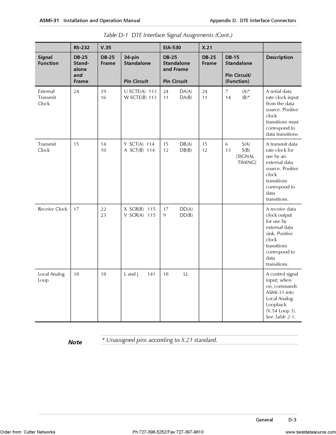
| Table | DTE Interface Signal Assignments (Cont.) |
|
|
| ||||||
|
|
|
|
|
|
|
|
|
|
|
|
|
| |
|
| V.35 |
|
|
| X.21 |
|
|
|
| ||||
|
|
|
|
|
|
|
|
|
|
|
|
| ||
Signal |
|
|
| Description | ||||||||||
Function |
| Stand- | Frame | Standalone | Standalone | Frame | Standalone |
|
| |||||
|
| alone |
|
|
|
|
| and Frame |
|
|
|
|
| |
|
| and |
|
|
|
|
|
|
|
| Pin Circuit/ |
|
| |
|
| Frame |
|
| Pin Circuit | Pin Circuit |
| (Function) |
|
| ||||
|
|
|
|
|
|
|
|
|
|
|
|
|
| |
External |
| 24 | 19 | U SCTE(A) | 113 | 24 | DA(A) | 24 | 7 | (A)* | A serial data | |||
Transmit |
|
| 16 | W SCTE(B) 113 | 11 | DA(B) | 11 | 14 | (B)* | rate clock input | ||||
Clock |
|
|
|
|
|
|
|
|
|
|
|
| from the data | |
|
|
|
|
|
|
|
|
|
|
|
|
| source. Positive | |
|
|
|
|
|
|
|
|
|
|
|
|
| clock | |
|
|
|
|
|
|
|
|
|
|
|
|
| transitions must | |
|
|
|
|
|
|
|
|
|
|
|
|
| correspond to | |
|
|
|
|
|
|
|
|
|
|
|
|
| data transitions. | |
|
|
|
|
|
|
|
|
|
|
|
|
|
|
|
Transmit |
| 15 | 14 | Y | SCT(A) | 114 | 15 | DB(A) | 15 | 6 | S(A) | A transmit data | ||
Clock |
|
| 10 | A | SCT(B) | 114 | 12 | DB(B) | 12 | 13 | S(B) | rate clock for | ||
|
|
|
|
|
|
|
|
|
|
|
| [SIGNAL | use by an | |
|
|
|
|
|
|
|
|
|
|
|
| TIMING] | external data | |
|
|
|
|
|
|
|
|
|
|
|
|
| source. Positive | |
|
|
|
|
|
|
|
|
|
|
|
|
| clock | |
|
|
|
|
|
|
|
|
|
|
|
|
| transitions | |
|
|
|
|
|
|
|
|
|
|
|
|
| correspond to | |
|
|
|
|
|
|
|
|
|
|
|
|
| data | |
|
|
|
|
|
|
|
|
|
|
|
|
| transitions. | |
|
|
|
|
|
|
|
|
|
|
|
|
|
|
|
Receive Clock |
| 17 | 22 | X | SCR(B) | 115 | 17 | DD(A) |
|
|
| A receive data | ||
|
|
| 23 | V SCR(A) | 115 | 9 | DD(B) |
|
|
| clock output | |||
|
|
|
|
|
|
|
|
|
|
|
|
| for use by | |
|
|
|
|
|
|
|
|
|
|
|
|
| external data | |
|
|
|
|
|
|
|
|
|
|
|
|
| sink. Positive | |
|
|
|
|
|
|
|
|
|
|
|
|
| clock | |
|
|
|
|
|
|
|
|
|
|
|
|
| transitions | |
|
|
|
|
|
|
|
|
|
|
|
|
| correspond to | |
|
|
|
|
|
|
|
|
|
|
|
|
| data | |
|
|
|
|
|
|
|
|
|
|
|
|
| transitions. | |
|
|
|
|
|
|
|
|
|
|
|
|
|
| |
Local Analog |
| 18 | 18 | L and j | 141 | 18 | LL |
|
|
| A control signal | |||
Loop |
|
|
|
|
|
|
|
|
|
|
|
| input; when | |
|
|
|
|
|
|
|
|
|
|
|
|
| on, commands | |
|
|
|
|
|
|
|
|
|
|
|
|
| ||
|
|
|
|
|
|
|
|
|
|
|
|
| Local Analog | |
|
|
|
|
|
|
|
|
|
|
|
|
| Loopback | |
|
|
|
|
|
|
|
|
|
|
|
|
| (V.54 Loop 3). | |
|
|
|
|
|
|
|
|
|
|
|
|
| See Table | |
|
|
|
|
|
|
|
|
|
|
|
| |||
|
|
|
|
|
|
|
|
| ||||||
| Note |
| * Unassigned pins according to X.21 standard. |
|
|
|
| |||||||
General
Order from: Cutter Networks | www.bestdatasource.com |