Appendix C. X.21 Interface Module

ASMi-31Installation and Operation Manual


IR-X.21B

TXD


ETC


MODEM


RXC


FIFO


Buffer


RXD


Rx


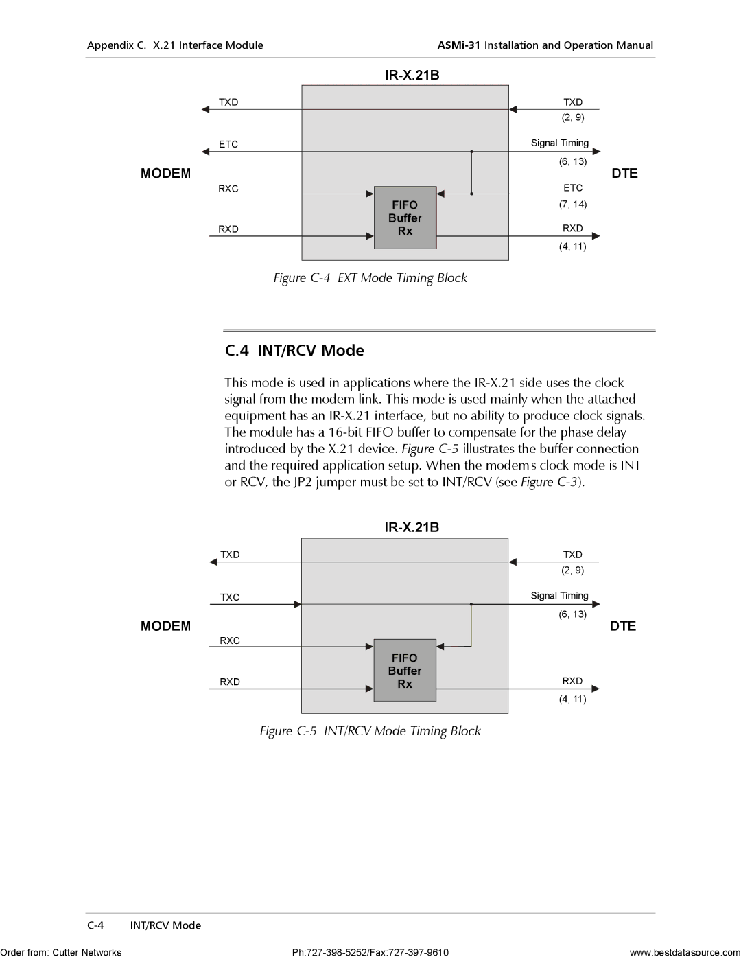
Figure C-4 EXT Mode Timing Block

TXD (2, 9)

Signal Timing (6, 13)

DTE

ETC (7, 14)

RXD

(4, 11)

C.4 INT/RCV Mode

This mode is used in applications where the IR-X.21 side uses the clock signal from the modem link. This mode is used mainly when the attached equipment has an IR-X.21 interface, but no ability to produce clock signals. The module has a 16-bit FIFO buffer to compensate for the phase delay introduced by the X.21 device. Figure C-5illustrates the buffer connection and the required application setup. When the modem's clock mode is INT or RCV, the JP2 jumper must be set to INT/RCV (see Figure C-3).

TXD

TXC

MODEM

RXC

RXD

IR-X.21B

FIFO

Buffer

Rx

TXD (2, 9)

Signal Timing

(6, 13)

DTE

RXD

(4, 11)

Figure C-5 INT/RCV Mode Timing Block

C-4 INT/RCV Mode

Order from: Cutter Networks

Ph:727-398-5252/Fax:727-397-9610

www.bestdatasource.com

Page 56
Image 56
RAD Data comm ASMi-31 operation manual Figure C-4 EXT Mode Timing Block, Figure C-5 INT/RCV Mode Timing Block