Chapter 4 – SocketModem Parallel Interface – A Programmer’s Description
FIFO Operation
The
Receive (RX) FIFO
The RX FIFO can be configured to be 16 words deep and 11 bits wide. Each word in the RX FIFO consists of 8 data bits and 3 error bits. The RX block of the MMM contains read and write pointers and status flag circuitry that need only to be presented with data (for input), reset, read/write control signals, and read/write clock signals. The RX block of the MMM internally manages the FIFO register file and pointers, and it provides simultaneous read/write capability (no contention problems).
The RX block of the MMM provides data (for output), FIFO full flag, FIFO empty flag, and an almost full flag which uses an associated predefined trigger level (obtained from the MMM FCR control register) to signal when the trigger level has been met. Four possible trigger levels may be selected by programming bits
A typical (interrupt driven) write to the RX block is a
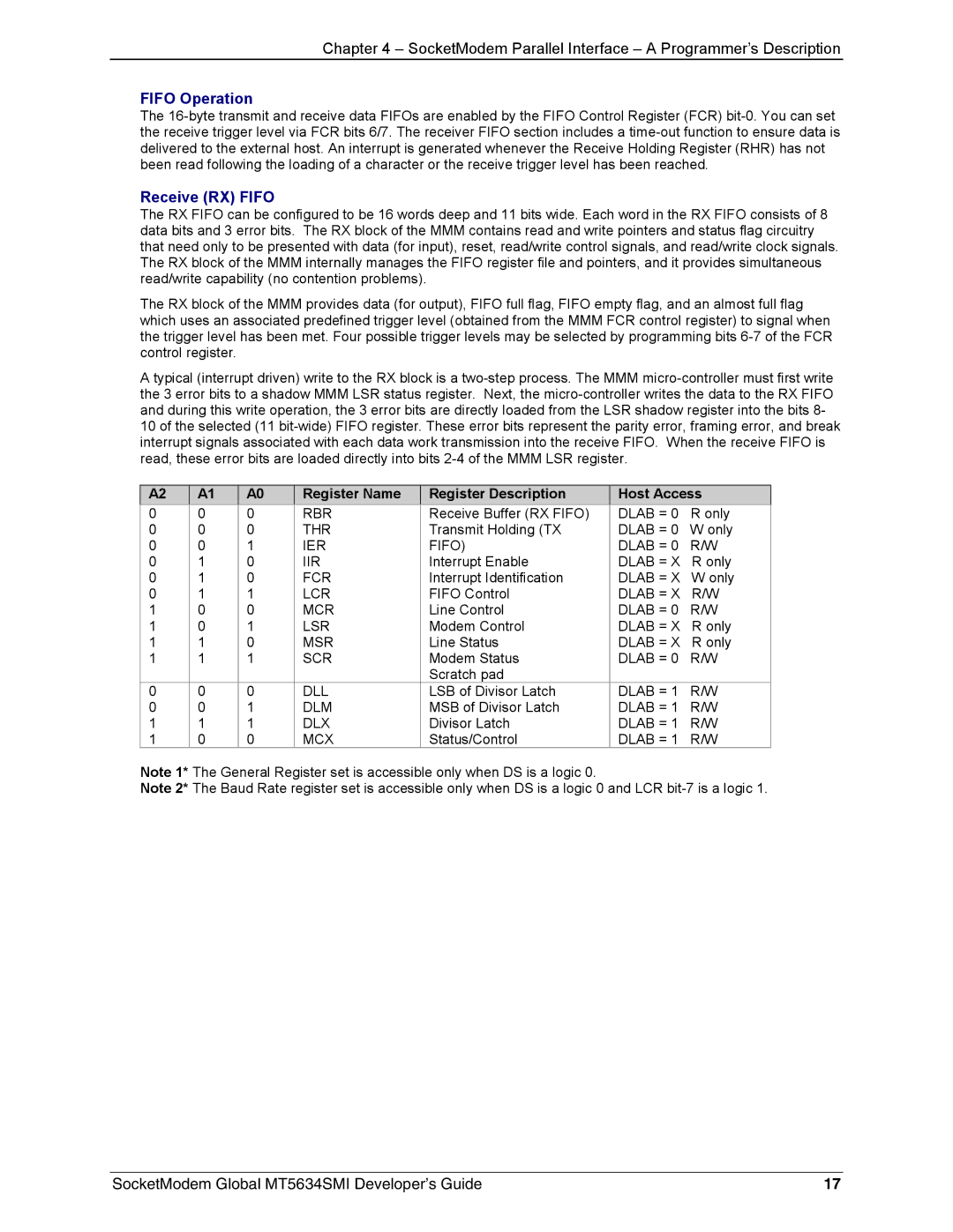
A2 | A1 | A0 | Register Name | Register Description | Host Access | |
0 | 0 | 0 | RBR | Receive Buffer (RX FIFO) | DLAB = 0 | R only |
0 | 0 | 0 | THR | Transmit Holding (TX | DLAB = 0 | W only |
0 | 0 | 1 | IER | FIFO) | DLAB = 0 | R/W |
0 | 1 | 0 | IIR | Interrupt Enable | DLAB = X | R only |
0 | 1 | 0 | FCR | Interrupt Identification | DLAB = X | W only |
0 | 1 | 1 | LCR | FIFO Control | DLAB = X | R/W |
1 | 0 | 0 | MCR | Line Control | DLAB = 0 | R/W |
1 | 0 | 1 | LSR | Modem Control | DLAB = X | R only |
1 | 1 | 0 | MSR | Line Status | DLAB = X | R only |
1 | 1 | 1 | SCR | Modem Status | DLAB = 0 | R/W |
|
|
|
| Scratch pad |
|
|
0 | 0 | 0 | DLL | LSB of Divisor Latch | DLAB = 1 | R/W |
0 | 0 | 1 | DLM | MSB of Divisor Latch | DLAB = 1 | R/W |
1 | 1 | 1 | DLX | Divisor Latch | DLAB = 1 | R/W |
1 | 0 | 0 | MCX | Status/Control | DLAB = 1 | R/W |
Note 1* The General Register set is accessible only when DS is a logic 0.
Note 2* The Baud Rate register set is accessible only when DS is a logic 0 and LCR
SocketModem Global MT5634SMI Developer’s Guide | 17 |