Chapter 4 – SocketModem Parallel Interface – A Programmer’s Description
Time Out Interrupts
The interrupts are enabled by IER bits
The LSR register provides the current singular highest priority interrupt only. A condition can exist where a higher priority interrupt may mask the lower priority interrupt(s). Only after servicing the higher pending interrupt will the lower priority interrupt(s) be reflected in the status register. Servicing the interrupt without investigating further interrupt conditions can result in data errors. When two interrupt conditions have the same priority, it is important to service these interrupts correctly.
Receive Data Ready and Receive Time Out have the same interrupt priority (when enabled by IER
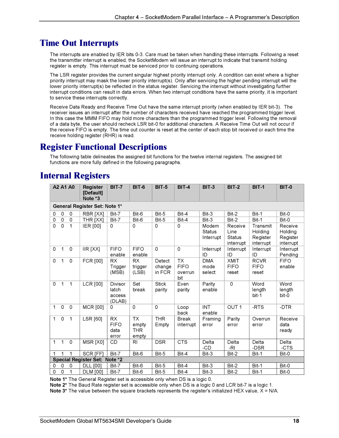
Register Functional Descriptions
The following table delineates the assigned bit functions for the twelve internal registers. The assigned bit functions are more fully defined in the following paragraphs.
Internal Registers
A2 A1 A0 | Register | ||||||||||
|
|
| [Default] |
|
|
|
|
|
|
|
|
|
|
| Note *3 |
|
|
|
|
|
|
|
|
General Register Set: Note 1* |
|
|
|
|
|
|
| ||||
0 | 0 | 0 | RBR [XX] | ||||||||
0 | 0 | 0 | THR [XX] | ||||||||
0 | 0 | 1 | IER [00] | 0 | 0 | 0 | 0 | Modem | Receive | Transmit | Receive |
|
|
|
|
|
|
|
| Status | Line | Holding | Holding |
|
|
|
|
|
|
|
| Interrupt | Status | Register | Register |
|
|
|
|
|
|
|
|
| interrupt | interrupt | interrupt |
0 | 1 | 0 | IIR [XX] | FIFO | FIFO | 0 | 0 | Interrupt | Interrupt | Interrupt | Interrupt |
|
|
|
| enable | enable |
|
| ID | ID | ID | Pending |
0 | 1 | 0 | FCR [00] | RX | RX | Detect | TX | DMA | XMIT | RCVR | FIFO |
|
|
|
| Trigger | trigger | change | FIFO | mode | FIFO | FIFO | enable |
|
|
|
| (MSB) | (LSB) | in FCR | overrun | select | reset | reset |
|
|
|
|
|
|
|
| bit |
|
|
|
|
0 | 1 | 1 | LCR [00] | Divisor | Set | Stick | Even | Parity | 0 | Word | Word |
|
|
|
| latch | break | parity | parity | enable |
| length | length |
|
|
|
| access |
|
|
|
|
| ||
|
|
|
| (DLAB) |
|
|
|
|
|
|
|
1 | 0 | 0 | MCR [00] | 0 | 0 | 0 | Loop | INT | OUT 1 |
| |
|
|
|
|
|
|
| back | enable |
|
|
|
1 0 1
LSR [60] RX FIFO data error
TX empty
THR empty
THR | Break | Framing | Parity |
Empty | interrupt | error | error |
|
|
|
|
Overrun error
Receive data ready
1 | 1 | 0 | MSR [X0] | CD | RI | DSR | CTS | Delta | Delta | Delta | Delta |
|
|
|
|
|
|
|
|
| |||
1 | 1 | 1 | SCR [FF] | ||||||||
Special Register Set: Note *2 |
|
|
|
|
|
|
| ||||
0 | 0 | 0 | DLL [00] | ||||||||
0 | 0 | 1 | DLM [00] | ||||||||
Note 1* The General Register set is accessible only when DS is a logic 0.
Note 2* The Baud Rate register set is accessible only when DS is a logic 0 and LCR
SocketModem Global MT5634SMI Developer’s Guide | 18 |