Chapter 4 – SocketModem Parallel Interface – A Programmer’s Description
FCR FIFO Control
Bits
Bit 5: Used to detect a change in the FCR.
Bit 4: TX FIFO overrun bit.
Bit 3: DMA mode select. If bit 3 is a 0, the 16450 mode is enabled which does only
Bit 2: TX FIFO reset. This will cause TX FIFO pointer logic to be reset (any data in TX FIFO will be lost). This bit is self clearing; however, a shadow bit exists that is cleared only when read by the host, thus allowing the host to monitor a FIFO reset.
Bit 1: RX FIFO reset. This will cause RX FIFO pointer logic to be reset (any data in RX FIFO will be lost). This bit is self clearing; however, a shadow bit exists that is cleared only when read by the host, thus allowing the host to monitor a FIFO reset.
Bit 0: FIFO enable. The host writes this bit to logic 1 to put the block in FIFO mode. This bit must be a 1 when writing other bits in this register or they will not be programmed. When this bit changes state, any data in the FIFOs or the RBR and THR registers will be lost and any pending interrupts are cleared.
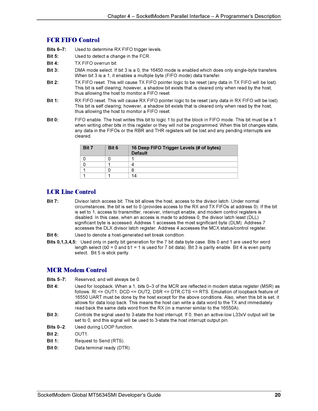
Bit 7 | Bit 6 | 16 Deep FIFO Trigger Levels (# of bytes) |
|
| Default |
0 | 0 | 1 |
0 | 1 | 4 |
1 | 0 | 8 |
1 | 1 | 14 |
LCR Line Control
Bit 7: Divisor latch access bit. This bit allows the host, access to the divisor latch. Under normal circumstances, the bit is set to 0 (provides access to the RX and TX FIFOs at address 0). If the bit is set to 1, access to transmitter, receiver, interrupt enable, and modem control registers is disabled. In this case, when an access is made to address 0, the divisor latch least (DLL) significant byte is accessed. Address 1 accesses the most significant byte (DLM). Address 7 accesses the DLX divisor latch register. Address 4 accesses the MCX status/control register.
Bit 6: Used to denote a
Bits 0,1,3,4,5: Used only in parity bit generation for the 7 bit data byte case. Bits 0 and 1 are used for word length select (b0 = 0 and b1 = 1 is used for 7 bit data). Bit 3 is parity enable. Bit 4 is even parity select. Bit 5 is stick parity.
MCR Modem Control
Bits | Reserved, and will always be 0. |
Bit 4: | Used for loopback. When a 1, bits |
| follows: RI <= OUT1, DCD <= OUT2, DSR <= DTR,CTS <= RTS. Emulation of loopback feature of |
| 16550 UART must be done by the host except for the above conditions. Also, when this bit is set, it |
| allows for data loop back. This means the host can write a data word to the TX and immediately |
| read back the same data word from the RX (in a manner similar to the 16550A). |
Bit 3: | Controls the signal used to |
| set to 0, and this signal will be used to |
Bits | Used during LOOP function. |
Bit 2: | OUT1. |
Bit 1: | Request to Send (RTS). |
Bit 0: | Data terminal ready (DTR). |
SocketModem Global MT5634SMI Developer’s Guide | 20 |