VXI Technology, Inc.
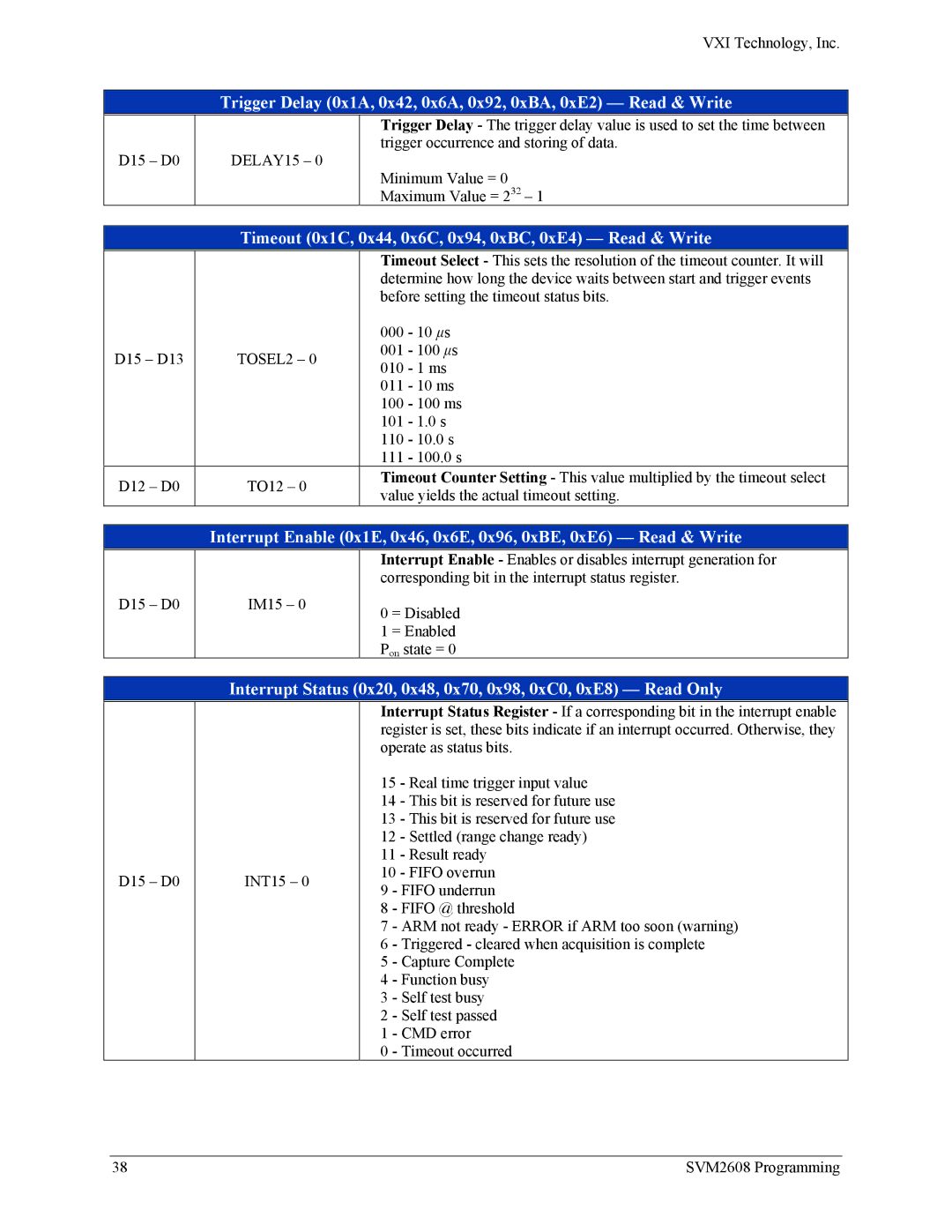
Trigger Delay (0x1A, 0x42, 0x6A, 0x92, 0xBA, 0xE2) — Read & Write
D15 – D0
DELAY15 – 0
Trigger Delay - The trigger delay value is used to set the time between trigger occurrence and storing of data.
Minimum Value = 0
Maximum Value = 232 – 1
Timeout (0x1C, 0x44, 0x6C, 0x94, 0xBC, 0xE4) — Read & Write
|
| Timeout Select - This sets the resolution of the timeout counter. It will | ||
|
| determine how long the device waits between start and trigger events | ||
|
| before setting the timeout status bits. | ||
|
| 000 | - 10 μs | |
D15 – D13 | TOSEL2 – 0 | 001 | - 100 μs | |
010 | - 1 ms | |||
|
| |||
|
| 011 | - 10 ms | |
|
| 100 | - 100 ms | |
|
| 101 | - 1.0 s | |
|
| 110 | - 10.0 s | |
|
| 111 | - 100.0 s | |
D12 – D0 | TO12 – 0 | Timeout Counter Setting - This value multiplied by the timeout select | ||
value yields the actual timeout setting. | ||||
|
| |||
Interrupt Enable (0x1E, 0x46, 0x6E, 0x96, 0xBE, 0xE6) — Read & Write
D15 – D0
IM15 – 0
Interrupt Enable - Enables or disables interrupt generation for corresponding bit in the interrupt status register.
0 = Disabled
1 = Enabled Pon state = 0
Interrupt Status (0x20, 0x48, 0x70, 0x98, 0xC0, 0xE8) — Read Only
D15 – D0
INT15 – 0
Interrupt Status Register - If a corresponding bit in the interrupt enable register is set, these bits indicate if an interrupt occurred. Otherwise, they operate as status bits.
15 - Real time trigger input value
14 - This bit is reserved for future use
13 - This bit is reserved for future use
12 - Settled (range change ready)
11 - Result ready
10 - FIFO overrun
9 - FIFO underrun
8 - FIFO @ threshold
7 - ARM not ready - ERROR if ARM too soon (warning) 6 - Triggered - cleared when acquisition is complete
5 - Capture Complete
4 - Function busy
3 - Self test busy
2 - Self test passed
1 - CMD error
0 - Timeout occurred
38 | SVM2608 Programming |
