31994A | AMD Sempron™ Processor Model 10 with 256K L2 Cache Data Sheet |
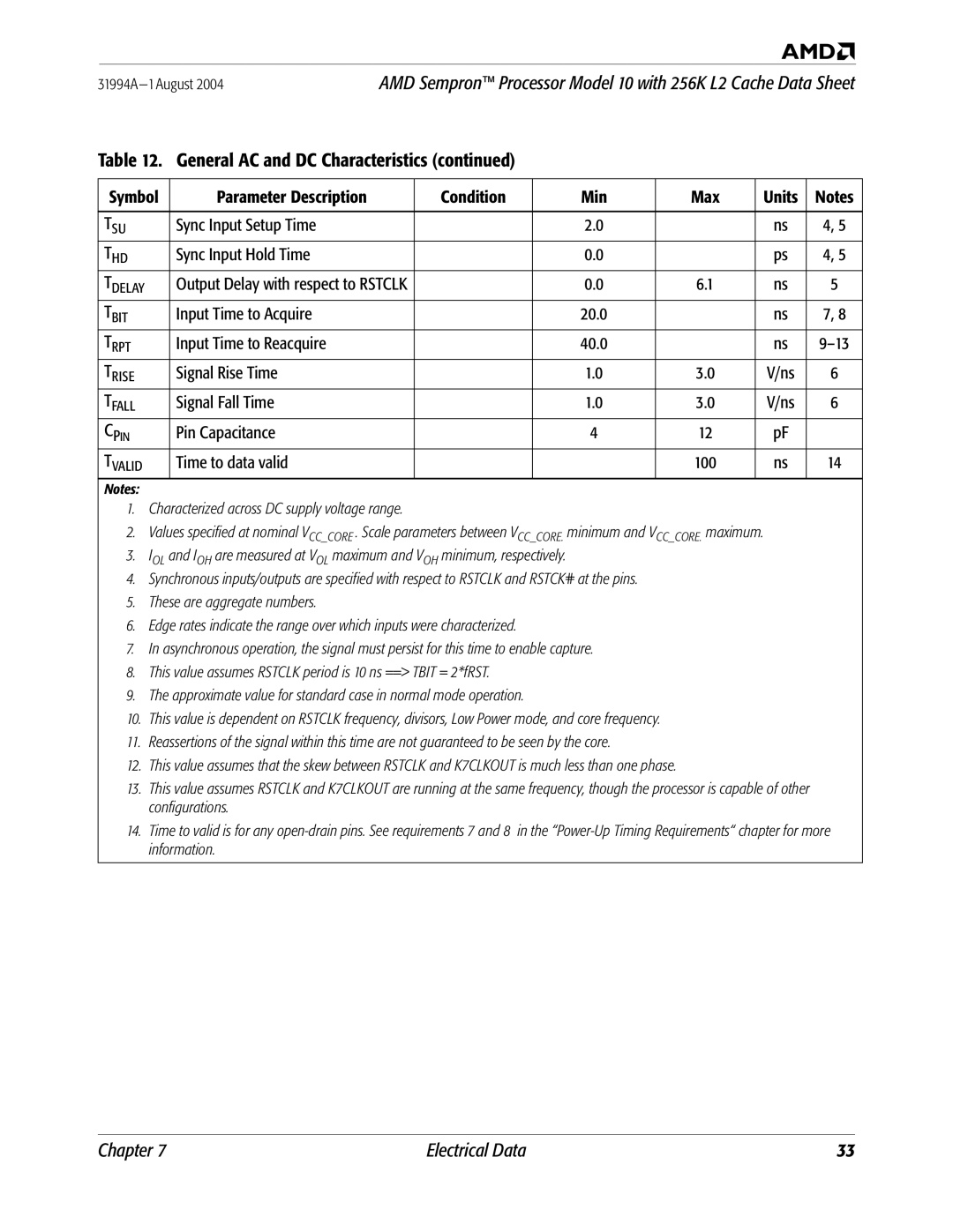
Table 12. General AC and DC Characteristics (continued)
Symbol | Parameter Description | Condition |
| Min |
| Max | Units |
| Notes | |
|
|
|
|
|
|
|
|
|
|
|
TSU |
| Sync Input Setup Time |
|
| 2.0 |
|
| ns |
| 4, 5 |
THD |
| Sync Input Hold Time |
|
| 0.0 |
|
| ps |
| 4, 5 |
TDELAY |
| Output Delay with respect to RSTCLK |
|
| 0.0 |
| 6.1 | ns |
| 5 |
TBIT |
| Input Time to Acquire |
|
| 20.0 |
|
| ns |
| 7, 8 |
TRPT |
| Input Time to Reacquire |
|
| 40.0 |
|
| ns |
| |
TRISE |
| Signal Rise Time |
|
| 1.0 |
| 3.0 | V/ns |
| 6 |
TFALL |
| Signal Fall Time |
|
| 1.0 |
| 3.0 | V/ns |
| 6 |
CPIN |
| Pin Capacitance |
|
| 4 |
| 12 | pF |
|
|
TVALID |
| Time to data valid |
|
|
|
| 100 | ns |
| 14 |
Notes: |
|
|
|
|
|
|
|
|
|
|
1. | Characterized across DC supply voltage range. |
|
|
|
|
|
|
|
| |
2. | Values specified at nominal VCC_CORE . Scale parameters between VCC_CORE. minimum and VCC_CORE. maximum. |
| ||||||||
3. | IOL and IOH are measured at VOL maximum and VOH minimum, respectively. |
|
|
|
| |||||
4. | Synchronous inputs/outputs are specified with respect to RSTCLK and RSTCK# at the pins. |
|
|
|
| |||||
5. | These are aggregate numbers. |
|
|
|
|
|
|
|
| |
6. | Edge rates indicate the range over which inputs were characterized. |
|
|
|
|
|
|
| ||
7. | In asynchronous operation, the signal must persist for this time to enable capture. |
|
|
|
| |||||
8. | This value assumes RSTCLK period is 10 ns ==> TBIT = 2*fRST. |
|
|
|
|
|
|
| ||
9. | The approximate value for standard case in normal mode operation. |
|
|
|
| |||||
10. | This value is dependent on RSTCLK frequency, divisors, Low Power mode, and core frequency. |
|
|
|
| |||||
11. | Reassertions of the signal within this time are not guaranteed to be seen by the core. |
|
|
|
| |||||
12. | This value assumes that the skew between RSTCLK and K7CLKOUT is much less than one phase. |
|
|
|
| |||||
13. | This value assumes RSTCLK and K7CLKOUT are running at the same frequency, though the processor is capable of other |
| ||||||||
| configurations. |
|
|
|
|
|
|
|
| |
14. | Time to valid is for any | in the | ||||||||
| information. |
|
|
|
|
|
|
|
| |
|
|
|
|
|
|
|
|
|
|
|
Chapter 7 | Electrical Data | 33 |