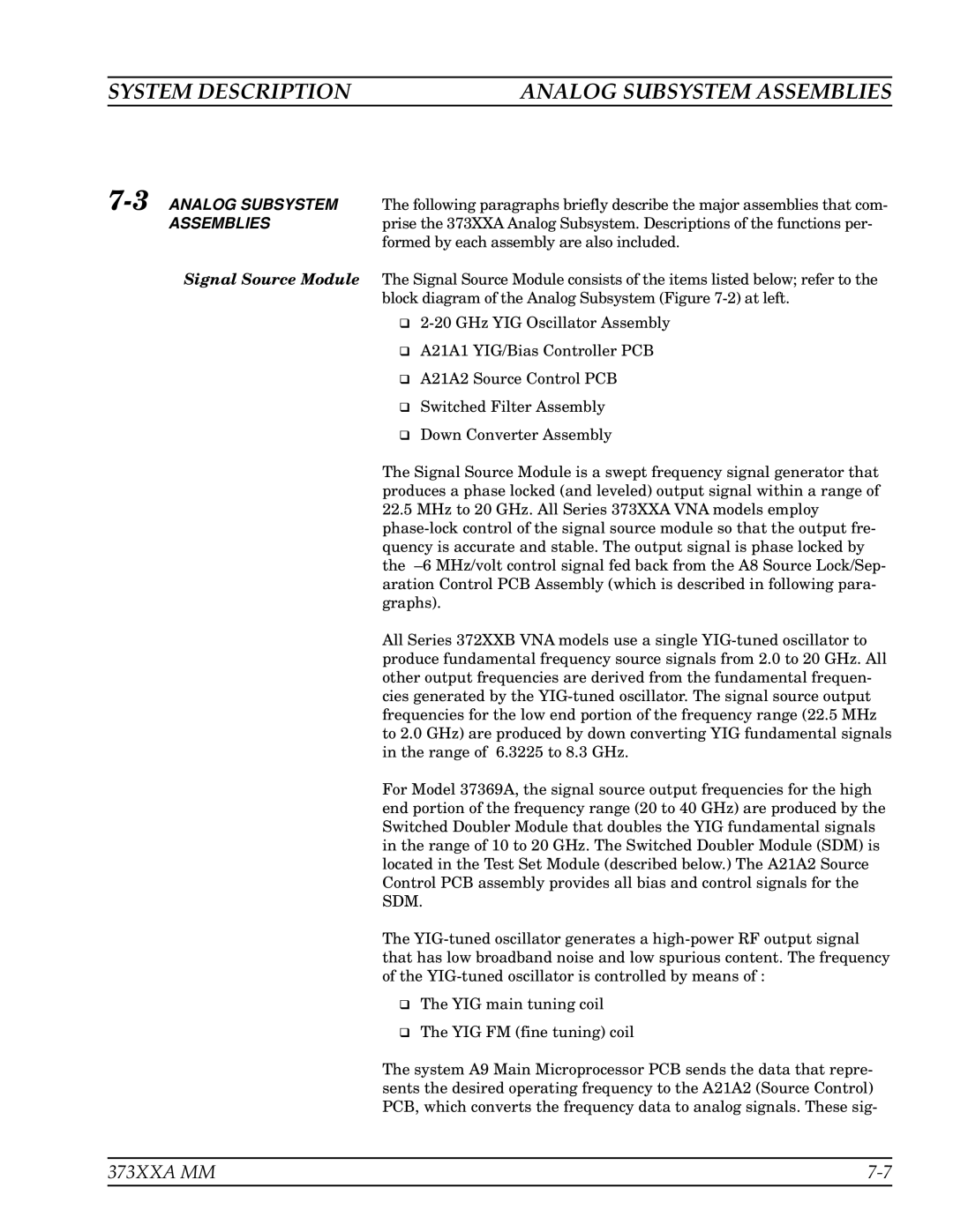
Anritsu 373XXA manual Analog Subsystem Assemblies, 3ANALOG Subsystem, Signal Source Module, Sdm

Models: 373XXA

1 202
Download 202 pages 15.37 Kb
Page 102
Image 102

SYSTEM DESCRIPTION

ANALOG SUBSYSTEM ASSEMBLIES

7-3ANALOG SUBSYSTEM

The following paragraphs briefly describe the major assemblies that com-

ASSEMBLIES

prise the 373XXA Analog Subsystem. Descriptions of the functions per-


formed by each assembly are also included.

Signal Source Module

The Signal Source Module consists of the items listed below; refer to the


block diagram of the Analog Subsystem (Figure 7-2) at left.


￿ 2-20 GHz YIG Oscillator Assembly


￿ A21A1 YIG/Bias Controller PCB


￿ A21A2 Source Control PCB


￿ Switched Filter Assembly


￿ Down Converter Assembly


The Signal Source Module is a swept frequency signal generator that


produces a phase locked (and leveled) output signal within a range of


22.5 MHz to 20 GHz. All Series 373XXA VNA models employ


phase-lock control of the signal source module so that the output fre-


quency is accurate and stable. The output signal is phase locked by


the –6 MHz/volt control signal fed back from the A8 Source Lock/Sep-


aration Control PCB Assembly (which is described in following para-


graphs).


All Series 372XXB VNA models use a single YIG-tuned oscillator to


produce fundamental frequency source signals from 2.0 to 20 GHz. All


other output frequencies are derived from the fundamental frequen-


cies generated by the YIG-tuned oscillator. The signal source output


frequencies for the low end portion of the frequency range (22.5 MHz


to 2.0 GHz) are produced by down converting YIG fundamental signals


in the range of 6.3225 to 8.3 GHz.


For Model 37369A, the signal source output frequencies for the high


end portion of the frequency range (20 to 40 GHz) are produced by the


Switched Doubler Module that doubles the YIG fundamental signals


in the range of 10 to 20 GHz. The Switched Doubler Module (SDM) is


located in the Test Set Module (described below.) The A21A2 Source


Control PCB assembly provides all bias and control signals for the


SDM.

The YIG-tuned oscillator generates a high-power RF output signal that has low broadband noise and low spurious content. The frequency of the YIG-tuned oscillator is controlled by means of :

￿The YIG main tuning coil

￿The YIG FM (fine tuning) coil

The system A9 Main Microprocessor PCB sends the data that repre- sents the desired operating frequency to the A21A2 (Source Control) PCB, which converts the frequency data to analog signals. These sig-

373XXA MM

7-7

Page 102
Image 102
Anritsu 373XXA manual Analog Subsystem Assemblies, 3ANALOG Subsystem, Signal Source Module, Sdm

373XXA specifications

The Anritsu 373XXA series is a notable line of microwave and RF signal analyzers designed for comprehensive analysis and testing of various wireless communication technologies. These analyzers are specifically crafted to meet the demands of modern communication systems, making them ideal for engineers and technicians working in wireless research, development, and manufacturing.

One of the main features of the Anritsu 373XXA series is its wide frequency range, which typically spans from as low as 5 kHz to several GHz, accommodating a vast array of signal types and applications. This extensive frequency coverage allows users to test and validate all manner of systems, from LTE and 5G networks to satellite communications, yielding accurate and reliable measurement results.

The device employs advanced measurement technologies that provide in-depth analysis capabilities. Among these technologies is the ability to perform both time and frequency domain measurements, allowing users to visualize and diagnose signal integrity issues effectively. In addition, the 373XXA series incorporates vector signal analysis, which is crucial in evaluating complex modulated signals, commonly found in today’s sophisticated wireless communication protocols.

Another distinguishing characteristic of the Anritsu 373XXA is its user-friendly interface. It features a large, high-resolution display that enables easy navigation through the analyzer's functions and measurements. The intuitive design is further enhanced by customizable settings and measurement configurations that streamline the workflow, making it accessible for both novice and experienced users.

The 373XXA series also supports various digital and analog signal demodulation techniques, ensuring compatibility with an array of communication standards. Furthermore, users can benefit from its built-in signal generation capabilities, which allows for end-to-end testing of devices and systems under realistic operational conditions.

Portability is another key feature of the Anritsu 373XXA series. The compact design and lightweight structure facilitate easy transport, which is particularly advantageous for field applications where mobility is critical.

Overall, the Anritsu 373XXA series stands out as a versatile and powerful tool for professionals in the RF and microwave field, thanks to its extensive frequency range, advanced measurement technologies, user-friendly interface, and portability. Whether developing new wireless standards or troubleshooting existing systems, the 373XXA delivers precision and reliability essential for today’s dynamic communication landscape.