Definity Communications System
Page
Contents
Multiplexing Outside the Switch
Communication System Networking AN Overview
Tandem TIE Trunk Networks
Distributed Communications System DCS
Data Connectivity AN Overview
Special Data Features
Data Communications Capabilities
Data Communications Configurations
Related Documents Synchronization of Digital Facilities
Trunking Terms and Capabilities Communications Protocols
Glossary
Index
List of Figures
DSU
Mpdm
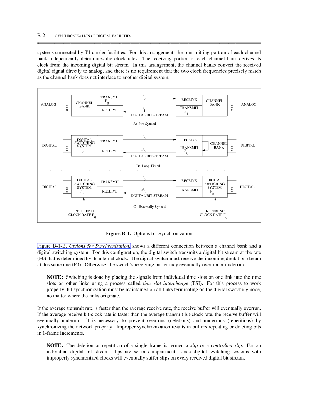
Figure B-1 Options for Synchronization
Figure B-11 External and Internal Reference Levels
List of Tables
BCC
EIA RS-449 V.24 LEADS/DEFINITIONS
EIA RS-232C V.28 LEADS/DEFINITIONS
EIA RS-232D V.28 LEADS/DEFINITIONS
EIA RS-366 LEADS/DEFINITIONS
Xvi Contents
About this Document
Prerequisite Skills and Knowledge
Document Organization
Part
∙ Glossary ∙ Index
HOW to Make Comments about this Document
AT&T
Xx about this Document
Introduction to Connectivity
2INTRODUCTION to Connectivity
Transmission Types
Analog Transmission
Digital Transmission
Analog-to-Digital Conversion
Analog VS. Digital
6TRANSMISSION Types
Entering the Switch
Transmission States
Voice Transmission
8TRANSMISSION States Digital Switch
Exiting the Switch
⎜ Module
Circuit Packs
Data Transmission
Protocol Layers
12TRANSMISSION States Originating Switch Destination
Protocols Used
Layer 1 Protocols
Layer 2 Protocols
Protocol States
⎜DMI Mode Code
Connectivity Rules
16TRANSMISSION States
Frequency-Division Multiplexing
Multiplexed Communication
Types of Multiplexing
Time-Division Multiplexing
Statistical Multiplexing
Multiplexing Over DS1 Facilities
Line Coding
Alternating Mark Inversion
Zero Code Suppression ZCS Line Coding
B8ZS Line Coding
Signal Inversion
Restricted ⎜ Unrestricted
⎜ DMI
7Data-Module Capabilities Part 2
D4 Framing
Framing
Signaling
D4 Framing
ESF Framing
Robbed-Bit Signaling
ESF
24th-Channel Signaling
⎜ Channels 24th Channel ⎜ 24th Channel
⎜ Frame No
Trunk Types/Destinations ⎜ Signaling Types
⎜ DMI-BOS
⎜ Isdn PRI
Multiplexing Outside the Switch
Multiplexing onto T1 Trunks
CDM CEM Host Digital DMI PBX
Compressing the Signal
Getting the Signal Ready for the Central Office
Altering Channel Assignments on T1 Trunks
DR23N DR18M DR18W DR23W
Multiplexing with Microwave
Microwave System T1 Trunk Capacity
Demultiplexing
10.Possible Multiplexed Connections
Statistical Multiplexing
Trunking
Application
Local Exchange Trunks
Tie Trunks
Miscellaneous Trunks
Special-Access Trunks
Auxiliary Trunks
Release Link Trunks RLTs
Advanced Private Line Termination Aplt Trunks
Remote Access Trunks
Host-Access Trunks
Connectivity
Administration Options
System 85/G2 Administration
Signaling Types
Signaling Protocols
Trunk Type
Group Type
System 75/G1 Administration
Comm Type
DS1 Options
Interface Circuit
Trunk Tables
Trunking
44TRUNKING
11.Generic 1 and Generic 2 Digital Trunks Voice BCC
46TRUNKING
Trunking
48TRUNKING
Trunking
50TRUNKING
Trunking
52TRUNKING
Communication System Networking AN Overview
Types of Networks
Network Evolution
DCS
Software ⎜ Network Type S75/G1 S85/G2 Package
PEC
Software Capabilities
System 75 and Generic 1 UDP Package
DIMENSION, System 85, and Generic 2 Multipremises Package
System 75 and Generic 1 PNA Package
Distributed Communications System
Network Call Processing
Internal Dial Plan
Uniform Numbering
Routing the Call
DAC + EXT To ARS
Auxiliary Call Information
Automatic Alternate Routing
Selecting a Routing Pattern
∙ RNX
∙ The FRL of the call
∙ Where the trunk group appears in the list of preferences
Selecting a Trunk Group
Modifying the Digits
Automatic Route Selection
Analyzing the Dialed Number
Communication System Networking AN Overview To AAR
Selecting the Routing Pattern
Network Administration
Networking Feature Parameters
Private Network Trunks
⎜ Maap ⎜ Vmaap
System Definity Feature PBX
20COMMUNICATION System Networking AN Overview
Tandem TIE Trunk Networks
Interactions with Other Networks
2TANDEM TIE Trunk Networks
Attendant Lines ⎜ Main Satellite ⎜ Trunks
MS/T Configurations
Main-Satellite Configuration
Main-Tributary Configuration
MS/T Features
Networking Package Multipremises with ETA
Main Networking Package PNA, ETN
Routing Incoming Calls
Routing Outgoing Calls
Other Routing Capabilities
Engineering Considerations
Interactions
Page
ETN Configurations
ETN Trunks
Page
Access and Bypass Access Tie Trunks
Features
Off-Net Trunks
Uniform Numbering Plan
Attendant
ETN Interactions with Other Networks
Extension Number Portability Clusters
Software-Defined Network
Call Routing SDN to ETN
Call Routing ETN to SDN
Release Link Trunk Networks CAS and ACD
Centralized Attendant Service
Automatic Call Distribution
Distributed Communications System Clusters
Main-Satellite/Tributary Networks
Distributed Communications System DCS
Switch Node Capacity
DCS Clusters
DCS Links
Signaling Link Speed
Signaling Links
Switch Physical Links ⎜Logical Channels/Link
Signaling Link Protocol
Transmission Media
Direct Link DCS Connections
Linkage Design
Distributed Communications System DCS
MTDM/MPDM
DCS Signaling Link Connections
Equipment Distance Limitation
System 75 or Generic 1 G1 to System 75 or G1
System 75/G1 Signaling Channel DCP
Mtdm
System 85 or Generic 2 G2 to System 85 or G2
Modem
System 75 or Generic 1 G1 to System 85 or Generic 2 G2
RS232C to RS449 Conversion Dciu
Transparent Attendant Features
Dimension Signaling Links
Transparent Features
Attendant Call Waiting
Alphanumeric Display
Attendant Control of Trunk Group Access
⎜ ACA
Automatic Circuit Assurance
Busy Verification of Terminal Lines
Class-of-Service/Restriction Display
Trunk Group Busy/Warning Indicators
Calling Number Display
Transparent Voice Terminal Features
Alerting-Distinctive Ringing
Automatic Callback on Busy or No Answer
Call Waiting
Call Coverage Tone
Call Forwarding
Leave Word Calling LWC Without AP
Audio Information Exchange Audix Features Transparency
Call Transfer/Conference
20.AUDIX in a DCS Network
Definity PBX ⎜ Feature
22DISTRIBUTED Communications System DCS
Administration Considerations
Distributed Communications System, Issue 3
Dimension PBX
Data Connectivity AN Overview
Data Communications Variables
Communications Protocols
Digital PBX Public Switched Network Pooled Modem
Analog vs. Digital
Synchronous vs. Asynchronous
∙ ∙ ∙
Simplex vs. Half-Duplex vs. Full-Duplex
Parallel vs. Serial
Transmission Speed
Creating Switch Packet vs. Circuit Switches
Type of Communications Channel
Channel Information Bearer vs. Signaling Channels
Transmission Mode Changes and Modem Pools
Channel Assignment Dial-up vs. Dedicated Connections
Special Data Features
Terminal Dialing
Computer Dialing
⎜Data Services Features
Data Call Setup From a Voice Terminal
Data Hot Line
Data Restriction
Data Protection
Data Privacy
Data Only Off-Premises Extension
Off-Premises Data-Only Extension Configurations
Data Communications Capabilities
2DATA Communications Capabilities
DTE Connections
DTE Compatibility
Protocol Converters
Terminal Emulators
PC/PBX or PC/ISDN
DCE Possibilities
Data Modules
Voice Terminal Adjunct Data Modules
ADUs
Data Module Characteristics
Standalone Data Modules
Modems
DTE Connections
Dtdm
ADM
⎜ PC/PBX
PC/PBX
PC/ISDN
Modem Pooling Connections
DCP TIP-RING
12DTE Connections Data Module
Local Area Network Connections
LAN Topology
LAN Protocol
LAN Connectors
LAN Transmission Media
Advantages of a Communications System in a LAN Environment
LAN
LAN
Access to/from LANs That Use Other Operating Systems
Type Operating Gateway PC
System Software
Local Area Network Connections Remote PC
ISN Communication
Communication Between the LAN and Other Networks
X.25 Router
Type Operating Communications
System Package
SNA Gateway
Communication System as a LAN Backup
12.LAN/SNA Connectivity
Public and Private Data Network Connections
Accunet Packet Service
APS Access
Public Data Networks
Circuit-Switched Public Data Networks
SDS and Sddn Applications
Public and Private Data Network Connections
MPDM/M1
Public and Private Data Network Connections DTE Mpdm
Private Data Networks
Terrestrial Private Data Network Links
Private Connections Through Accunet T1.5 and T45
MPDM/M1* AMI
28PUBLIC and Private Data Network Connections
⎜AMI
Satellite Private Data Network Links
Telemarketing Host Connections
Isdn Gateway
Integrated Telemarketing Gateway
22.Telemarketing Gateway Configuration
For further details, see
34TELEMARKETING Host Connections
Data Network Administration
36DATA Network Administration
Data Communications Configurations
DSC and PSC Connections
DSC
4DATA Communications Configurations
SNA Node Connections
Connections Through Public or Private Data Networks
File Transfers
Video Teleconferencing
Image Processing
FAX Transmittal
8DATA Communications Configurations
Operation
Related Documents
General
Reference
2RELATED Documents
Related Documents
Dimension
Administration
System 75 and Generic
6RELATED Documents
Service
Sales
System 85 and Generic
8RELATED Documents
Sales
10RELATED Documents
Synchronization of Digital Facilities
Need for Synchronization
Figure B-1.Options for Synchronization
Synchronization Hierarchy
4SYNCHRONIZATION of Digital Facilities
Synchronization of Digital Facilities
∙ DDS
Figure B-3.Stratum Levels for the Synchronization Hierarchy
System 85 and Generic 2 Synchronization Architecture
Page
Primary
RED YEL Good LOS Misf
Primary Secondary Reference Indicators ⎜ Reference
⎜ Indicators
⎜ Blue RED
System 75 and Generic 1 Synchronization Architecture
Figure B-6.Tone-Clock Synchronizer Nonduplicated, Generic
System 75 and Generic 1 Synchronization Software Operation
Criteria for Switching to the Secondary Reference
Criteria for Switching Back to the Primary Reference
External Synchronization Clock
CROSS-CONNECT B25A Cable
Output
Figure B-9.External-Clock Interface
Selecting a Timing Source for the Switch
Network Synchronization and Engineering
Internal Reference Selection Rules
Rule
Example for Rule
Figure B-13.Proper Use of Backup Facilities
Page
Figure B-15.Optimal Diverse Routing
Figure B-16.Less Than Optimal Diverse Routing
Figure B-17.Excessive Cascading
Figure B-19.Excessive Synchronization from One Node
External-Reference Selection Rules
Rules 2 Through
Availability of Synchronization Sources
Misconception
Fact
USE of Generic 2 AS a System Clock Reference
Line-Only Mode DS1/DMI-BOS ANN11 or TN767
Conclusions on Synchronization
ISDN-PRI Trunk Facilities
USE of Generic 1 AS a System Clock Reference
Line+Trunk Mode DS1/DMI-BOS ANN35 or TN767 with TN555
DMI-MOS ANN35 or TN767 with TN555
Trunk-Mode ISDN-PRI TN767
Line-Only Mode DS1/DMI-BOS TN767
Trunk-Mode Interface ISDN-PRI + Robbed Bit TN767
Trunk-Mode DS1/DMI-MOS TN767
32SYNCHRONIZATION of Digital Facilities
Trunking Terms and Capabilities
Wire Tie Trunk
Address Signaling
Frequently Used Terms
Auto or Automatic-incoming
Alerting Signals
APLT-Advanced Private Line Termination
Auto or Automatic-outgoing
Customer Provided Access
Ccsa or Common Control Switching Arrangement
CX Signaling or Composite Signaling
Cut-Through Mode of Operation
Delay-Dial Outgoing
Delay-Dial
Delay-Dial Incoming
Delay-Dial Start-Dial Ddsd
Dial Repeating Tie Trunk
Derived E&M Lead Signaling
Designed Trunks
Dial-Pulse
Lead Signaling or Ear & Mouth Signaling
Direct Access
Epscs or Enhanced Private Switched Communications Service
Standard or Type 1A and Type I compatible or Type 1B
ETN Trunking Facilities
FX or Foreign Exchange
Glare Resolution
Glare
Glare Detection
Immediate Start
Ground Start
High-Usage Trunk Group
Immediate Start Incoming
Intermachine Trunk IMT
Interdigit Time-out
Intermediate High-Usage Trunk Group
Intertandem Trunk
Main PBX
Out-of-Band Signaling
Party Test Signal
Main-Satellite Trunks
Senderized Mode of Operation
Reverse Battery
SF or Single Frequency signaling
Signal Converter
Stop-Go Signaling
Signaling Type
Special Access Connections
Supervisory Signaling
Type of Dialing
Touch-Tone Signaling
Trunk Type or trunk group type
Type of Outpulsing
Wats Wide Area Telephone Service Trunk
Wink-Start Incoming
Wink-Start Outgoing
Suggestions and Helpful Hints
Trunking Characteristics Table
Signaling Types
System 85, or Dimension PBX
Switch a
Supervision Signaling Tion Generic
⎜GROUP/CALL Type
Switch B
GROUP/CALL Type
DOD
23/FX-DOD OUT
IN/DID
GROUP/CALL Type Signaling
26/WATS
27/WATS OUT
28/WATS-DOD OUT
⎜⎜ E&M
35/TIE
ESS 5ESS ⎜OTHER
⎜ LS ⎜ RB
⎜ System 85, or ⎜DIMENSION PBX ⎜
⎜57/CAS RLT-OUTGOING From Branch ⎜66/CAS RLT-INCOMING
Main Satellite
⎜DIAL-TONE with
Analog Data Modem Side
Digital Data ⎜DATA Module Side 103/HOST Access
Line Side 104/HOST Access
Trunk Side
Other
32TRUNKING Terms and Capabilities
Communications Protocols
Data-Link Layer
OSI Model
Physical Layer
Network Layer
Page
Figure D-1.OSI Reference Model
Application Layer
Session Layer
Presentation Layer
Standard Protocols
Table D-1.Some Ccitt Digital Standards
Table D-2.Some Ccitt Analog Standards
Ccitt X.26 RS-423A FED-STD
Table D-2.Some Ccitt Analog Standards
Other Common Standards
CCITT-ISO
AT&T Protocols
EIA
Data Mode Capabilities
Digital Multiplexed Interface
Data Modes
Applications
Description
Control Data DCP DS1/DMI/BOS Channel
14COMMUNICATIONS Protocols
Communications Protocols Flag
Digital Communications Protocol
Or multipoint
BX.25
Communication Pathways and Endpoints
Message, Packet, and Frame
Sldh
Lead Definitions
SBA
SCF
SCB
SBB
RL/CG
CH/CI
RDA
SDA
STA
RSA
CRQ
DPR
ACR
PND
DDA
BBA
BBB
DDB
⎜ PIN
8LEAD Definitions
Networking FEATURES--AVAILABILITY Matrix
⎜⎜ R1
Networking FEATURES--AVAILABILITY Matrix Contd
⎜ NA
⎜ Uniform Numbering ⎜ Plan Note
6NETWORKING FEATURES--AVAILABILITY Matrix
Abbreviations
CSU
CRC
CSM
DAC
FAX
ETA
ETN
FEP
Mtdm
Mpdm
MS/T
NCP
SNA
SDN
SMT
Teho
AB-6ABBREVIATIONS
ADM
Glossary
ACU
AVD
ADS
Automatic Alternate
Also high-volume tandem
Audix Standalone
Routing AAR
Bit-oriented signaling
Service Bccos
Bipolar signal
Message-oriented signaling
BSC
Ccitt
CPU
COS
Ccis
COR
CPE
See network channel-terminating equipment
See data communications equipment
DCS cluster DCS node
Dciu link
DCP DCS
See bit rate
DDC
DDD
See digital telephone
DMI/MOS
DCS DMI-BOS
DMI-MOS
DS1
Communications systems and switch
Error-free second
ESS electronic switching
Framing format Extended trunk access
BX.25 DCIU/PI
Hdlc
Keyboard dialing Kilo bits per second kbps
LAN Lapd
See basic rate interface See primary rate interface
Also wide area network
Listed directory number
Local area network LAN
Local exchange company
Ncte
NAU
PAD
PVC
PDM
Robbed-bit signaling
921, and signaling system number
Remote access trunk
Protocol converter PC
Sdlc
TDM
UCD
UNP
Wats Wide Area
Service Wats trunk
Telecommunications Service
Telecommunications
Index
ARS 2-4,2-7,2-8,2-14plan
Bypass access trunk 1-37,4-7,4-8,5-1,5-4,C-2
IN-2 Index
Logical 6-3,D-19restricted 1-20unrestricted
Channel bank 1-9,1-10,1-29,1-30,B-20frame
Dial access code 2-2,2-5,2-10,2-13,2-17,3-1,4-4
CRC 1-25CSMA/CD 8-13CSU
DAC 2-2,2-5,2-10,2-13,2-17,3-1,4-4,4-7,4-8,4-9,6-23
DMI 1-14, D-11
Mode 1-15,1-16,1-42,2-13,9-1MOS
6digitizer
DS1-Contd
FRL 2-10, 2-13
D4 1-24, 1-27
ESF 1-24, 1-27
Gateway 7-2
DCS 1-36,2-3,5-14
Statistical 1-17,1-18,1-34
LOS B-9,B-13 LWC 6-18,6-21,6-24
ETN 1-36,2-2,2-8,3-1,4-1,5-1,6-1
Analog 1-7,9-2trunk
PAD 7-2,8-21
PCM 1-5,1-7,1-14,1-18,B-1
DS1 1-13,1-16,1-18
PRI 1-13, D-11
RS-232C1-13,D-9
Physical layer 1-11,1-15,D-2,D-9
RS-232C1-13,6-3
1-39, C-3, C-5, C-6
RNX 2-10
Subnet trunking 2-11, 2-14, 4-9
Intelligent main 2-4, 4-4, 4-7
TCM 2-11,6-23
Analog 1-3,7-2,7-4 Bypass access 1-37,4-7,4-8,5-1,5-4
T1 carrier 1-6,1-18,1-32
final 5-2,C-9
Uniform numbering 2-8, 5-1, 5-5
Uniform dial plan 2-5, 2-8, 2-9
Analog 1-9
Auxiliary 1-10, 1-35
IN-12 Index