Ultra37000 CPLD Family
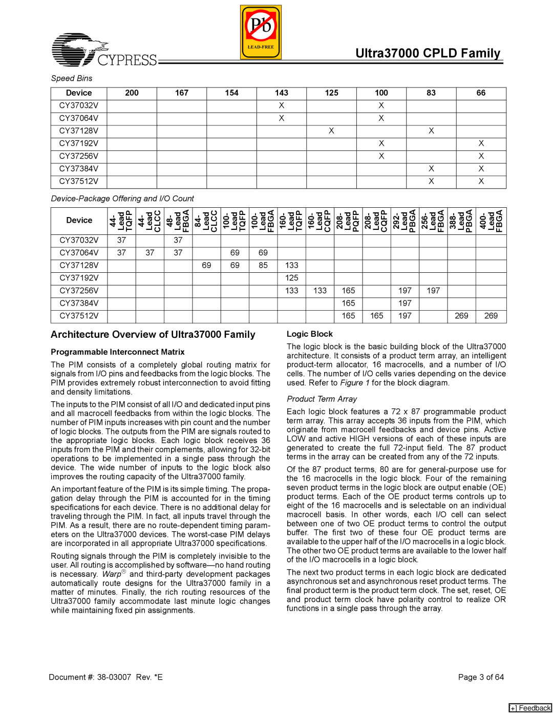
Speed Bins
Device | 200 |
| 167 |
|
| 154 |
|
| 143 | 125 |
| 100 |
|
| 83 |
|
| 66 | |||
CY37032V |
|
|
|
|
|
|
|
|
|
| X |
|
|
| X |
|
|
|
|
|
|
|
|
|
|
|
|
|
|
|
|
|
|
|
|
|
|
|
|
|
|
|
|
CY37064V |
|
|
|
|
|
|
|
|
|
| X |
|
|
| X |
|
|
|
|
|
|
|
|
|
|
|
|
|
|
|
|
|
|
|
|
|
|
|
|
|
|
|
|
CY37128V |
|
|
|
|
|
|
|
|
|
|
| X |
|
|
|
|
| X |
|
|
|
|
|
|
|
|
|
|
|
|
|
|
|
|
|
|
|
|
|
|
|
|
|
CY37192V |
|
|
|
|
|
|
|
|
|
|
|
|
|
| X |
|
|
|
|
| X |
|
|
|
|
|
|
|
|
|
|
|
|
|
|
|
|
|
|
|
|
|
|
CY37256V |
|
|
|
|
|
|
|
|
|
|
|
|
|
| X |
|
|
|
|
| X |
|
|
|
|
|
|
|
|
|
|
|
|
|
|
|
|
|
|
|
|
|
|
CY37384V |
|
|
|
|
|
|
|
|
|
|
|
|
|
|
|
|
| X |
|
| X |
|
|
|
|
|
|
|
|
|
|
|
|
|
|
|
|
|
|
|
|
|
|
CY37512V |
|
|
|
|
|
|
|
|
|
|
|
|
|
|
|
|
| X |
|
| X |
|
|
|
|
|
|
|
|
|
|
|
|
|
|
|
|
|
|
|
|
|
|
|
|
|
|
|
|
|
|
|
|
|
|
|
|
| |||||||
|
|
|
|
|
|
|
|
|
|
|
|
|
|
|
| ||||||
Device | 44- Lead TQFP | 44- Lead CLCC | 48- Lead FBGA | 84- Lead CLCC | 100- Lead TQFP | 100- Lead FBGA |
| 160- Lead TQFP | 160- Lead CQFP | 208- Lead PQFP | 208- Lead CQFP | 292- Lead PBGA | 256- Lead FBGA | 388- Lead PBGA | 400- Lead FBGA | ||||||
|
|
|
|
|
|
|
|
|
|
|
|
|
|
|
|
|
|
|
|
| |
|
|
|
|
|
|
|
|
|
|
|
|
|
|
|
|
|
|
|
|
|
|
CY37032V | 37 |
|
| 37 |
|
|
|
|
|
|
|
|
|
|
|
|
|
|
|
|
|
|
|
|
|
|
|
|
|
|
|
|
|
|
|
|
|
|
|
|
|
| |
CY37064V | 37 | 37 |
| 37 |
|
| 69 | 69 |
|
|
|
|
|
|
|
|
|
|
|
| |
|
|
|
|
|
|
|
|
|
|
|
|
|
|
|
|
|
|
|
| ||
CY37128V |
|
|
|
| 69 | 69 | 85 |
| 133 |
|
|
|
|
|
|
|
|
|
| ||
|
|
|
|
|
|
|
|
|
|
|
|
|
|
|
|
|
|
|
|
|
|
CY37192V |
|
|
|
|
|
|
|
|
|
| 125 |
|
|
|
|
|
|
|
|
|
|
|
|
|
|
|
|
|
|
|
|
|
|
|
|
|
|
|
|
|
|
| |
CY37256V |
|
|
|
|
|
|
|
|
|
| 133 | 133 | 165 |
|
| 197 | 197 |
|
|
| |
|
|
|
|
|
|
|
|
|
|
|
|
|
|
|
|
|
|
|
|
| |
CY37384V |
|
|
|
|
|
|
|
|
|
|
|
| 165 |
|
| 197 |
|
|
|
| |
|
|
|
|
|
|
|
|
|
|
|
|
|
|
|
|
|
|
|
| ||
CY37512V |
|
|
|
|
|
|
|
|
|
|
|
| 165 |
| 165 | 197 |
| 269 | 269 | ||
|
|
|
|
|
|
|
|
|
|
|
|
|
|
|
|
|
|
|
|
|
|
Architecture Overview of Ultra37000 Family
Programmable Interconnect Matrix
The PIM consists of a completely global routing matrix for signals from I/O pins and feedbacks from the logic blocks. The PIM provides extremely robust interconnection to avoid fitting and density limitations.
The inputs to the PIM consist of all I/O and dedicated input pins and all macrocell feedbacks from within the logic blocks. The number of PIM inputs increases with pin count and the number of logic blocks. The outputs from the PIM are signals routed to the appropriate logic blocks. Each logic block receives 36 inputs from the PIM and their complements, allowing for
An important feature of the PIM is its simple timing. The propa- gation delay through the PIM is accounted for in the timing specifications for each device. There is no additional delay for traveling through the PIM. In fact, all inputs travel through the PIM. As a result, there are no
Routing signals through the PIM is completely invisible to the user. All routing is accomplished by
Logic Block
The logic block is the basic building block of the Ultra37000 architecture. It consists of a product term array, an intelligent
Product Term Array
Each logic block features a 72 x 87 programmable product term array. This array accepts 36 inputs from the PIM, which originate from macrocell feedbacks and device pins. Active LOW and active HIGH versions of each of these inputs are generated to create the full
Of the 87 product terms, 80 are for
The next two product terms in each logic block are dedicated asynchronous set and asynchronous reset product terms. The final product term is the product term clock. The set, reset, OE and product term clock have polarity control to realize OR functions in a single pass through the array.
Document #: | Page 3 of 64 |
[+] Feedback