|
|
|
|
|
|
|
|
|
|
|
|
|
| Ultra37000 CPLD Family |
| ||||||||||
|
|
|
|
|
|
|
|
|
|
|
|
|
|
|
|
|
|
|
|
|
|
|
|
|
|
|
|
|
|
|
|
|
|
|
|
|
|
|
|
|
|
|
|
|
|
|
|
|
| ||
|
| Parameter[11] |
|
| VX |
|
|
|
| Output |
|
|
| ||||||||||||
|
|
|
| 1.5V | VOH |
|
|
|
|
|
|
|
|
|
|
|
|
|
|
|
|
|
|
| |
|
|
|
|
|
|
|
|
|
|
|
|
|
|
|
|
|
|
|
|
|
|
| |||
|
|
|
|
|
|
|
|
|
|
|
|
|
|
|
|
|
|
|
|
|
|
|
|
| |
|
|
|
|
|
|
|
|
|
|
|
|
|
|
|
|
|
|
|
|
|
|
|
|
| |
|
|
|
|
|
| 0.5V |
|
|
|
|
|
|
|
|
|
|
|
| VX |
|
|
| |||
|
|
|
|
|
|
|
|
|
|
|
|
|
|
|
|
|
|
|
|
|
| ||||
|
|
|
|
|
|
|
|
|
|
|
|
|
|
|
|
|
|
|
|
|
| ||||
|
|
|
|
|
|
|
|
|
|
|
|
|
|
|
|
|
|
|
|
|
|
|
|
| |
|
|
|
|
|
|
|
|
|
|
|
|
|
|
|
|
|
|
|
|
|
|
|
|
|
|
|
|
|
|
|
|
|
|
|
|
|
|
|
|
|
|
|
|
|
|
|
|
|
|
|
|
|
| tER(+) |
|
| 2.6V | VOL | 0.5V |
|
|
|
|
|
|
|
|
|
|
|
|
| VX |
|
|
| |
|
|
|
|
|
|
|
|
|
|
|
|
|
|
|
|
|
|
|
| ||||||
|
|
|
|
|
|
|
|
|
|
|
|
|
|
|
|
|
|
|
|
|
| ||||
|
|
|
|
|
|
|
|
|
|
|
|
|
|
|
|
|
|
|
|
| |||||
|
|
|
|
|
|
|
|
|
|
|
|
|
|
|
|
|
|
|
|
|
| ||||
|
|
|
|
|
|
|
|
|
|
|
|
|
|
|
|
|
|
|
|
|
|
|
|
| |
|
|
|
|
|
|
|
|
|
|
|
|
|
|
|
|
|
|
|
|
|
|
|
|
| |
|
|
|
|
|
|
|
|
|
|
|
|
|
|
|
|
|
|
|
|
|
|
|
|
|
|
|
|
|
|
|
|
|
|
|
|
|
|
|
|
|
|
|
|
|
|
|
|
|
|
|
|
|
| tEA(+) |
|
| 1.5V |
|
|
|
|
|
|
|
|
|
|
|
|
|
|
|
| VOH |
|
|
|
|
|
|
|
|
|
|
|
|
|
|
|
|
|
|
|
|
|
|
|
|
|
| |||
|
|
|
|
|
| VX | 0.5V |
|
|
|
|
|
|
|
|
|
|
|
|
|
|
|
| ||
|
|
|
|
|
|
|
|
|
|
|
|
|
|
|
|
|
|
|
|
| |||||
|
|
|
|
|
|
|
|
|
|
|
|
|
|
|
|
|
|
|
|
|
| ||||
|
|
|
|
|
|
|
|
|
|
|
|
|
|
|
|
|
|
|
|
|
|
|
|
| |
|
|
|
|
|
|
|
|
|
|
|
|
|
|
|
|
|
|
|
|
|
|
|
|
| |
|
|
|
|
|
|
|
|
|
|
|
|
|
|
|
|
|
|
|
|
|
|
|
|
|
|
|
|
|
|
|
|
|
|
|
|
|
|
|
|
|
|
|
|
|
|
|
|
|
|
|
|
|
|
|
| Vthe | VX |
|
|
|
|
|
|
|
|
|
|
|
|
|
|
|
|
|
|
| |
|
|
|
|
|
|
|
|
|
|
|
|
|
|
|
|
|
|
|
|
|
|
| |||
|
|
|
|
|
|
|
|
|
|
|
|
|
|
|
|
|
|
|
|
|
|
|
|
| |
|
|
|
|
|
|
|
|
|
|
|
|
|
|
|
|
|
|
|
|
|
|
|
|
| |
|
|
|
|
|
| 0.5V |
|
|
|
|
|
|
|
|
|
|
|
|
| VOL |
|
|
| ||
|
|
|
|
|
|
|
|
|
|
|
|
|
|
|
|
|
|
|
|
|
|
| |||
|
|
|
|
|
|
|
|
|
|
|
|
|
|
|
|
|
|
|
|
|
| ||||
|
|
|
|
|
|
|
|
|
|
|
|
|
|
|
|
|
|
|
|
|
|
|
|
|
|
|
|
|
|
|
|
|
|
|
|
|
|
|
|
|
|
|
|
|
|
|
|
|
|
|
|
|
|
|
|
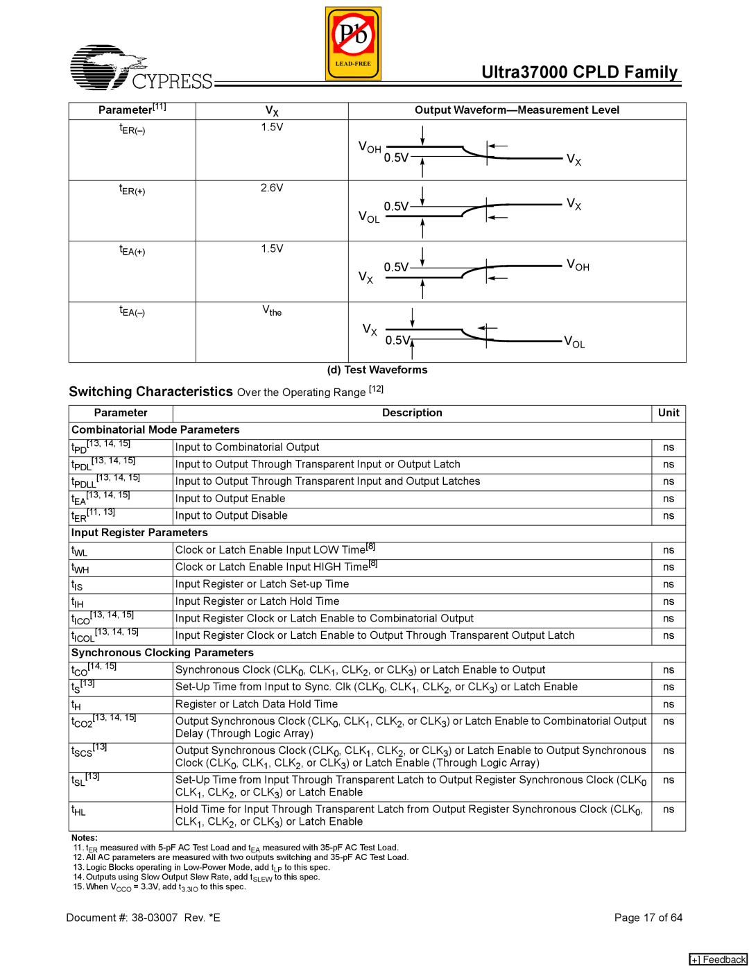
| (d) | Test Waveforms |
|
|
|
|
|
|
|
|
|
|
|
|
|
| |||||
Switching Characteristics Over the Operating Range [12] |
|
|
|
|
|
|
|
|
|
|
|
|
|
|
|
| |||||||||
|
| Parameter |
|
|
|
| Description |
|
|
|
|
|
|
|
|
|
|
|
| Unit |
| ||||
Combinatorial Mode | Parameters |
|
|
|
|
|
|
|
|
|
|
|
|
|
|
|
|
|
|
| |||||
|
|
|
|
|
|
|
|
|
|
|
|
|
|
|
|
|
|
|
|
| |||||
tPD[13, 14, 15] | Input to Combinatorial Output |
|
|
|
|
|
|
|
|
|
|
|
|
|
|
|
|
| ns |
| |||||
tPDL[13, 14, 15] | Input to Output Through Transparent Input or Output Latch |
|
|
|
|
|
|
|
|
|
| ns |
| ||||||||||||
tPDLL[13, 14, 15] | Input to Output Through Transparent Input and Output Latches |
|
|
|
|
|
|
|
|
|
| ns |
| ||||||||||||
t |
| [13, 14, 15] | Input to Output Enable |
|
|
|
|
|
|
|
|
|
|
|
|
|
|
|
|
| ns |
| |||
| EA |
|
|
|
|
|
|
|
|
|
|
|
|
|
|
|
|
|
|
|
|
|
|
| |
tER[11, 13] | Input to Output Disable |
|
|
|
|
|
|
|
|
|
|
|
|
|
|
|
|
| ns |
| |||||
Input Register Parameters |
|
|
|
|
|
|
|
|
|
|
|
|
|
|
|
|
|
|
| ||||||
|
|
|
|
|
|
|
|
|
|
|
|
|
|
|
|
|
|
|
|
| |||||
tWL | Clock or Latch Enable Input LOW Time[8] |
|
|
|
|
|
|
|
|
|
|
|
|
|
|
|
|
| ns |
| |||||
t | WH | Clock or Latch Enable Input HIGH Time[8] |
|
|
|
|
|
|
|
|
|
|
|
|
|
|
|
|
| ns |
| ||||
|
|
|
|
|
|
|
|
|
|
|
|
|
|
|
|
|
|
|
|
|
|
|
| ||
tIS |
| Input Register or Latch |
|
|
|
|
|
|
|
|
|
|
|
|
|
|
|
|
| ns |
| ||||
tIH |
| Input Register or Latch Hold Time |
|
|
|
|
|
|
|
|
|
|
|
|
|
|
|
|
| ns |
| ||||
tICO[13, 14, 15] | Input Register Clock or Latch Enable to Combinatorial Output |
|
|
|
|
|
|
|
|
|
| ns |
| ||||||||||||
tICOL[13, 14, 15] | Input Register Clock or Latch Enable to Output Through Transparent Output Latch |
| ns |
| |||||||||||||||||||||
Synchronous Clocking Parameters |
|
|
|
|
|
|
|
|
|
|
|
|
|
|
|
|
|
|
| ||||||
tCO[14, 15] | Synchronous Clock (CLK0, CLK1, CLK2, or CLK3) or Latch Enable to Output |
| ns |
| |||||||||||||||||||||
t | [13] |
| ns |
| |||||||||||||||||||||
| S |
| 0 |
|
| 1 |
| 2 |
| 3 |
|
|
|
|
|
|
|
|
| ||||||
tH |
| Register or Latch Data Hold Time |
|
|
|
|
|
|
|
|
|
|
|
|
|
|
|
|
| ns |
| ||||
tCO2[13, 14, 15] | Output Synchronous Clock (CLK0, CLK1, CLK2, or CLK3) or Latch Enable to Combinatorial Output | ns |
| ||||||||||||||||||||||
|
|
| Delay (Through Logic Array) |
|
|
|
|
|
|
|
|
|
|
|
|
|
|
|
|
|
|
| |||
tSCS[13] | Output Synchronous Clock (CLK0, CLK1, CLK2, or CLK3) or Latch Enable to Output Synchronous | ns |
| ||||||||||||||||||||||
|
|
| Clock (CLK0, CLK1, CLK2, or CLK3) or Latch Enable (Through Logic Array) |
|
|
| |||||||||||||||||||
t | SL | [13] | 0 | ns |
| ||||||||||||||||||||
|
| CLK1, CLK2, or CLK3) or Latch Enable |
|
|
|
|
|
|
|
|
|
|
|
|
|
|
|
|
|
| |||||
|
|
|
|
|
|
|
|
|
|
|
|
|
|
|
|
|
|
|
|
|
| ||||
tHL | Hold Time for Input Through Transparent Latch from Output Register Synchronous Clock (CLK0, | ns |
| ||||||||||||||||||||||
|
|
| CLK1, CLK2, or CLK3) or Latch Enable |
|
|
|
|
|
|
|
|
|
|
|
|
|
|
|
|
|
|
| |||
Notes: |
|
|
|
|
|
|
|
|
|
|
|
|
|
|
|
|
|
|
|
|
|
|
| ||
11.tER measured with
12.All AC parameters are measured with two outputs switching and
13.Logic Blocks operating in
14.Outputs using Slow Output Slew Rate, add tSLEW to this spec.
15.When VCCO = 3.3V, add t3.3IO to this spec.
Document #: | Page 17 of 64 |
[+] Feedback