CY7C1380D, CY7C1382D CY7C1380F, CY7C1382F
3.3V TAP AC Test Conditions
Input pulse levels |
|
|
|
|
| VSS to 3.3V | |||||||
Input rise and fall times |
|
|
|
|
| 1 ns | |||||||
Input timing reference levels |
|
|
| ........................ |
| 1.5V | |||||||
Output reference levels |
|
|
|
| 1.5V | ||||||||
Test load termination supply voltage | ................. |
|
|
|
| .............1.5V | |||||||
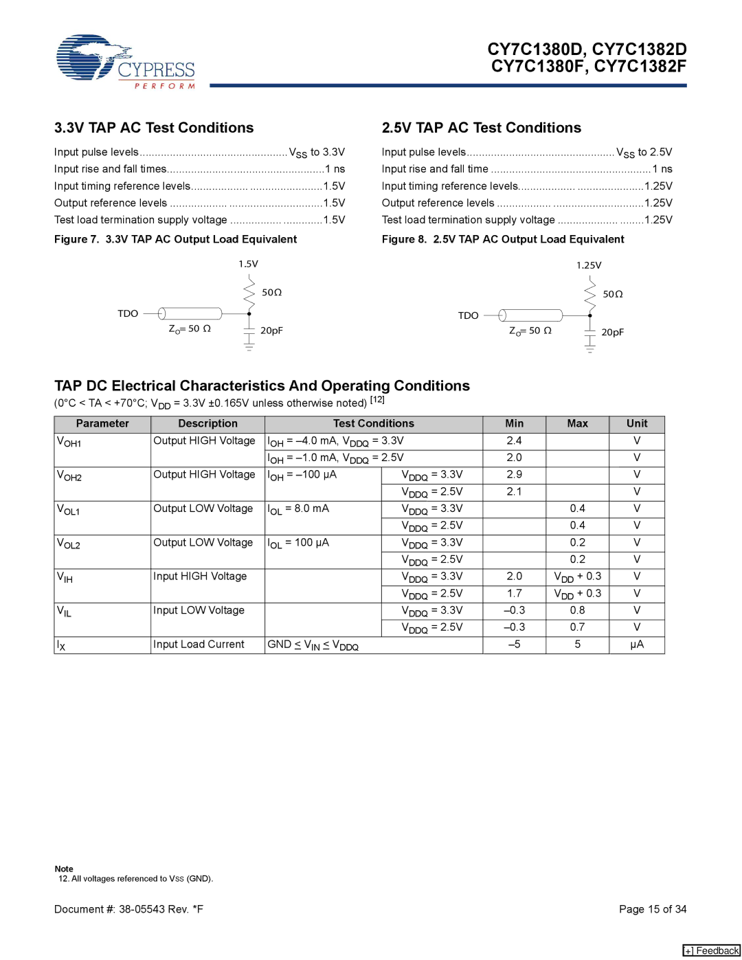
Figure 7. 3.3V TAP AC Output Load Equivalent | |||||||||||||
|
|
|
|
|
|
| 1.5V | ||||||
|
|
|
|
|
|
|
|
|
|
|
|
| 50Ω |
TDO |
|
|
|
|
|
|
|
|
|
|
|
|
|
|
|
|
|
|
|
|
|
|
|
|
| ||
|
|
|
|
|
|
|
|
|
|
|
|
| |
|
|
|
| ZO= 50 Ω |
|
|
|
|
|
| 20pF | ||
|
|
|
|
|
|
|
|
|
| ||||
|
|
|
|
|
|
|
|
|
|
|
|
|
|
|
|
|
|
|
|
|
|
|
|
|
|
|
|
|
|
|
|
|
|
|
|
|
|
|
|
|
|
2.5V TAP AC Test Conditions
Input pulse levels |
|
|
|
|
|
| VSS to 2.5V | ||||
Input rise and fall time |
|
|
|
|
|
| 1 ns | ||||
Input timing reference levels | ...................... |
|
|
|
| 1.25V | |||||
Output reference levels |
|
|
|
|
| 1.25V | |||||
Test load termination supply voltage |
|
|
|
|
|
| ........1.25V | ||||
Figure 8. 2.5V TAP AC Output Load Equivalent | |||||||||||
|
|
|
|
| 1.25V | ||||||
|
|
|
|
|
|
|
|
|
|
| 50Ω |
TDO |
|
|
|
|
|
|
|
|
|
|
|
|
|
|
|
|
|
|
|
| |||
|
|
|
|
|
|
|
|
|
|
| |
|
|
|
| ZO= 50 Ω |
|
|
|
|
|
| 20pF |
|
|
|
|
|
|
|
|
|
| ||
|
|
|
|
|
|
|
|
|
|
|
|
|
|
|
|
|
|
|
|
|
|
|
|
|
|
|
|
|
|
|
|
|
|
|
|
TAP DC Electrical Characteristics And Operating Conditions |
|
|
| ||||
(0°C < TA < +70°C; V = 3.3V ±0.165V unless otherwise noted) [12] |
|
|
|
| |||
| DD |
|
|
|
|
|
|
Parameter | Description | Test Conditions | Min | Max | Unit | ||
VOH1 | Output HIGH Voltage | IOH = | 2.4 |
| V | ||
|
| IOH = | 2.0 |
| V | ||
VOH2 | Output HIGH Voltage | IOH = |
| VDDQ = 3.3V | 2.9 |
| V |
|
|
|
| VDDQ = 2.5V | 2.1 |
| V |
VOL1 | Output LOW Voltage | IOL = 8.0 mA |
| VDDQ = 3.3V |
| 0.4 | V |
|
|
|
| VDDQ = 2.5V |
| 0.4 | V |
VOL2 | Output LOW Voltage | IOL = 100 µA |
| VDDQ = 3.3V |
| 0.2 | V |
|
|
|
| VDDQ = 2.5V |
| 0.2 | V |
VIH | Input HIGH Voltage |
|
| VDDQ = 3.3V | 2.0 | VDD + 0.3 | V |
|
|
|
| VDDQ = 2.5V | 1.7 | VDD + 0.3 | V |
VIL | Input LOW Voltage |
|
| VDDQ = 3.3V | 0.8 | V | |
|
|
|
| VDDQ = 2.5V | 0.7 | V | |
IX | Input Load Current | GND < VIN < VDDQ |
|
| 5 | µA | |
Note
12. All voltages referenced to VSS (GND).
Document #: | Page 15 of 34 |
[+] Feedback