|
|
|
|
|
|
|
| CY7C1380D, CY7C1382D | ||
|
|
|
|
|
|
|
| CY7C1380F, CY7C1382F | ||
|
|
|
|
|
|
|
|
|
|
|
|
|
|
|
|
|
|
|
|
| |
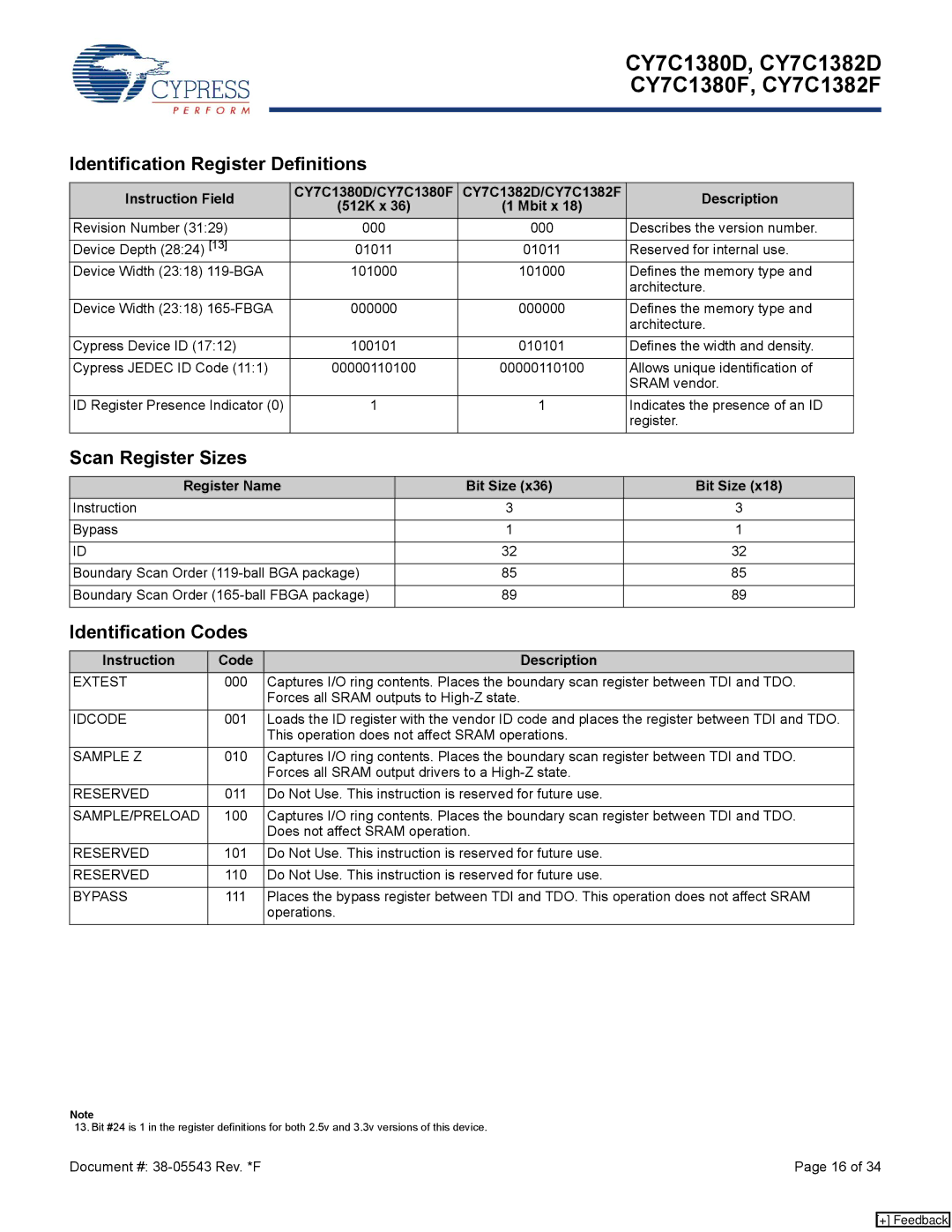
Identification Register Definitions |
|
|
|
| ||||||
|
|
|
|
|
|
|
|
|
|
|
Instruction Field |
|
|
| CY7C1380D/CY7C1380F | CY7C1382D/CY7C1382F | Description |
|
| ||
|
|
| (512K x 36) | (1 Mbit x 18) |
| |||||
|
|
|
|
|
|
|
| |||
Revision Number (31:29) |
|
|
| 000 |
| 000 | Describes the version number. |
|
| |
|
|
|
|
|
|
|
|
|
| |
Device Depth (28:24) [13] |
|
|
| 01011 |
| 01011 | Reserved for internal use. |
|
| |
Device Width (23:18) |
|
|
| 101000 | 101000 | Defines the memory type and |
|
| ||
|
|
|
|
|
|
|
| architecture. |
| |
Device Width (23:18) | 000000 | 000000 | Defines the memory type and |
|
| |||||
|
|
|
|
|
|
|
| architecture. |
| |
Cypress Device ID (17:12) |
|
|
| 100101 | 010101 | Defines the width and density. |
|
| ||
|
|
|
|
|
|
|
| |||
Cypress JEDEC ID Code (11:1) | 00000110100 | 00000110100 | Allows unique identification of |
|
| |||||
|
|
|
|
|
|
|
| SRAM vendor. |
| |
ID Register Presence Indicator (0) | 1 |
| 1 | Indicates the presence of an ID |
|
| ||||
|
|
|
|
|
|
|
| register. |
| |
Scan Register Sizes |
|
|
|
|
|
|
|
|
| |
|
|
|
|
|
|
|
| |||
Register Name |
|
| Bit Size (x36) | Bit Size (x18) |
|
| ||||
Instruction |
|
|
|
|
|
| 3 | 3 |
|
|
|
|
|
|
|
|
|
|
|
|
|
Bypass |
|
|
|
|
|
| 1 | 1 |
|
|
|
|
|
|
|
|
|
|
|
|
|
ID |
|
|
|
|
|
| 32 | 32 |
|
|
|
|
|
|
|
|
|
| |||
Boundary Scan Order |
| 85 | 85 |
|
| |||||
|
|
|
|
|
|
|
| |||
Boundary Scan Order |
| 89 | 89 |
|
| |||||
|
|
|
|
|
|
|
|
|
|
|
Identification Codes |
|
|
|
|
|
|
|
|
| |
|
|
|
|
|
|
|
|
|
|
|
Instruction | Code |
|
|
|
|
| Description |
|
|
|
EXTEST | 000 | Captures I/O ring contents. Places the boundary scan register between TDI and TDO. |
|
| ||||||
|
| Forces all SRAM outputs to |
|
|
| |||||
IDCODE | 001 | Loads the ID register with the vendor ID code and places the register between TDI and TDO. |
|
| ||||||
|
| This operation does not affect SRAM operations. |
|
|
| |||||
SAMPLE Z | 010 | Captures I/O ring contents. Places the boundary scan register between TDI and TDO. |
|
| ||||||
|
| Forces all SRAM output drivers to a |
|
|
| |||||
RESERVED | 011 | Do Not Use. This instruction is reserved for future use. |
|
|
| |||||
|
|
|
| |||||||
SAMPLE/PRELOAD | 100 | Captures I/O ring contents. Places the boundary scan register between TDI and TDO. |
|
| ||||||
|
| Does not affect SRAM operation. |
|
|
| |||||
RESERVED | 101 | Do Not Use. This instruction is reserved for future use. |
|
|
| |||||
|
|
|
|
|
| |||||
RESERVED | 110 | Do Not Use. This instruction is reserved for future use. |
|
|
| |||||
|
|
|
| |||||||
BYPASS | 111 | Places the bypass register between TDI and TDO. This operation does not affect SRAM |
|
| ||||||
|
| operations. |
|
|
|
| ||||
Note
13. Bit #24 is 1 in the register definitions for both 2.5v and 3.3v versions of this device.
Document #: | Page 16 of 34 |
[+] Feedback