CY7C1380D, CY7C1382D
CY7C1380F, CY7C1382F
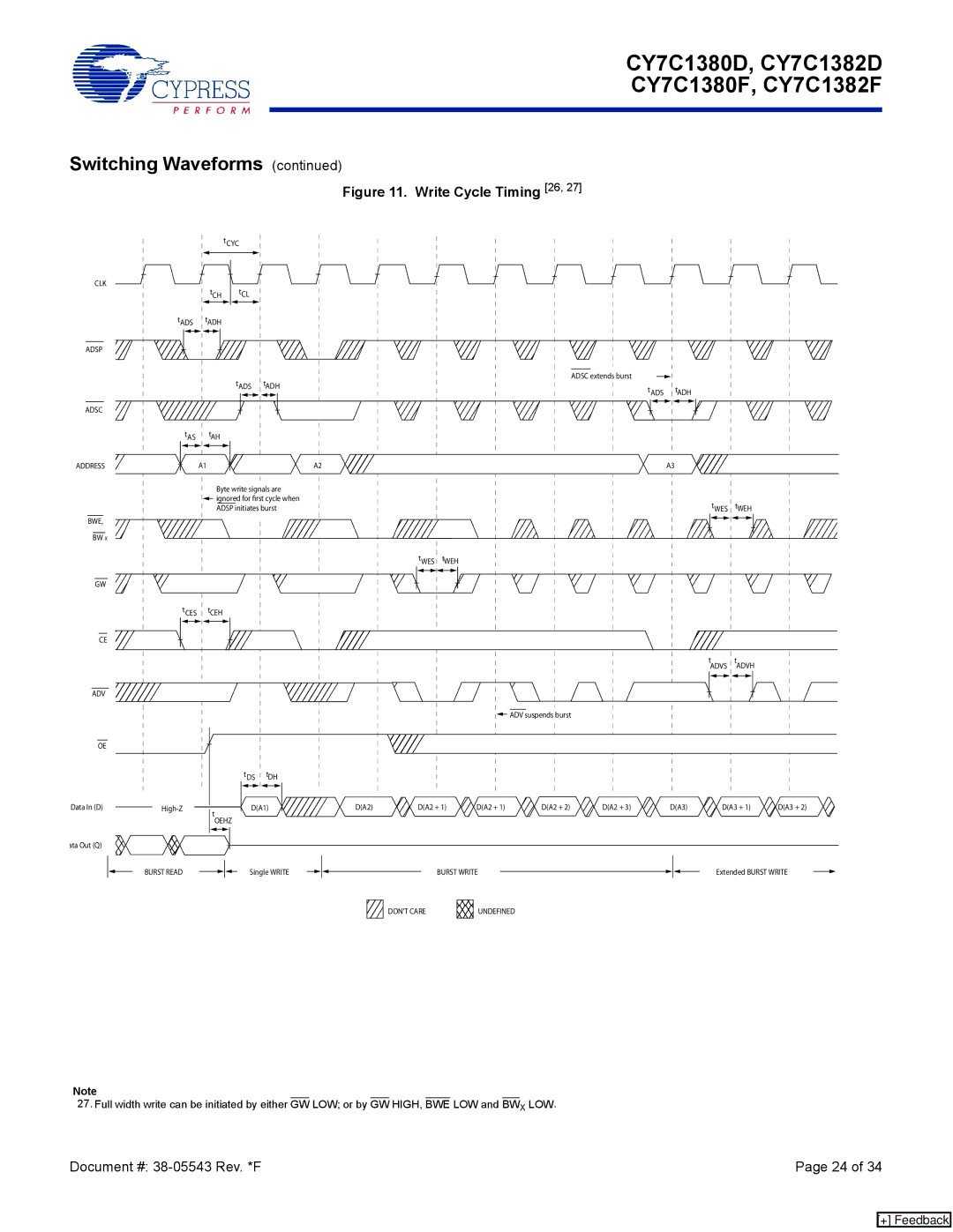
Switching Waveforms (continued)
Figure 11. Write Cycle Timing [26, 27]
|
|
| t CYC |
|
|
|
|
|
|
|
|
|
|
CLK |
| tCH | tCL |
|
|
|
|
|
|
|
|
|
|
|
|
|
|
|
|
|
|
|
|
|
| ||
| tADS | tADH |
|
|
|
|
|
|
|
|
|
|
|
ADSP |
|
|
|
|
|
|
|
|
|
|
|
|
|
|
|
| tADS | tADH |
|
|
|
| ADSC extends burst |
|
|
|
|
|
|
|
|
|
|
| tADS | tADH |
|
|
| ||
|
|
|
|
|
|
|
|
|
|
|
| ||
ADSC |
|
|
|
|
|
|
|
|
|
|
|
|
|
| tAS | tAH |
|
|
|
|
|
|
|
|
|
|
|
ADDRESS |
| A1 |
|
| A2 |
|
|
|
| A3 |
|
|
|
|
| Byte write signals are |
|
|
|
|
|
|
|
|
| ||
|
| ignored for first cycle when |
|
|
|
|
|
| tWES | tWEH |
| ||
|
| ADSP initiates burst |
|
|
|
|
|
|
| ||||
BWE, |
|
|
|
|
|
|
|
|
|
|
|
|
|
BW X |
|
|
|
|
|
|
|
|
|
|
|
|
|
|
|
|
|
|
| tWES tWEH |
|
|
|
|
|
|
|
GW |
|
|
|
|
|
|
|
|
|
|
|
|
|
| tCES | tCEH |
|
|
|
|
|
|
|
|
|
|
|
CE |
|
|
|
|
|
|
|
|
|
|
|
|
|
|
|
|
|
|
|
|
|
|
|
| tADVS | tADVH |
|
ADV |
|
|
|
|
|
|
|
|
|
|
|
|
|
|
|
|
|
|
|
|
| ADV suspends burst |
|
|
|
|
|
OE |
|
|
|
|
|
|
|
|
|
|
|
|
|
|
|
| tDS | tDH |
|
|
|
|
|
|
|
|
|
Data In (D) | t | D(A1) | D(A2) | D(A2 + 1) | D(A2 + 1) | D(A2 + 2) | D(A2 + 3) | D(A3) | D(A3 + 1) | D(A3 + 2) | |||
|
|
|
|
|
|
|
|
|
|
|
|
| |
|
| OEHZ |
|
|
|
|
|
|
|
|
|
| |
ata Out (Q) |
|
|
|
|
|
|
|
|
|
|
|
|
|
BURST READ
Single WRITE
BURST WRITE
Extended BURST WRITE
DON’T CARE
UNDEFINED
Note
27. Full width write can be initiated by either GW LOW; or by GW HIGH, BWE LOW and BWX LOW.
Document #: | Page 24 of 34 |
[+] Feedback