CY7C1380D, CY7C1382D
CY7C1380F, CY7C1382F
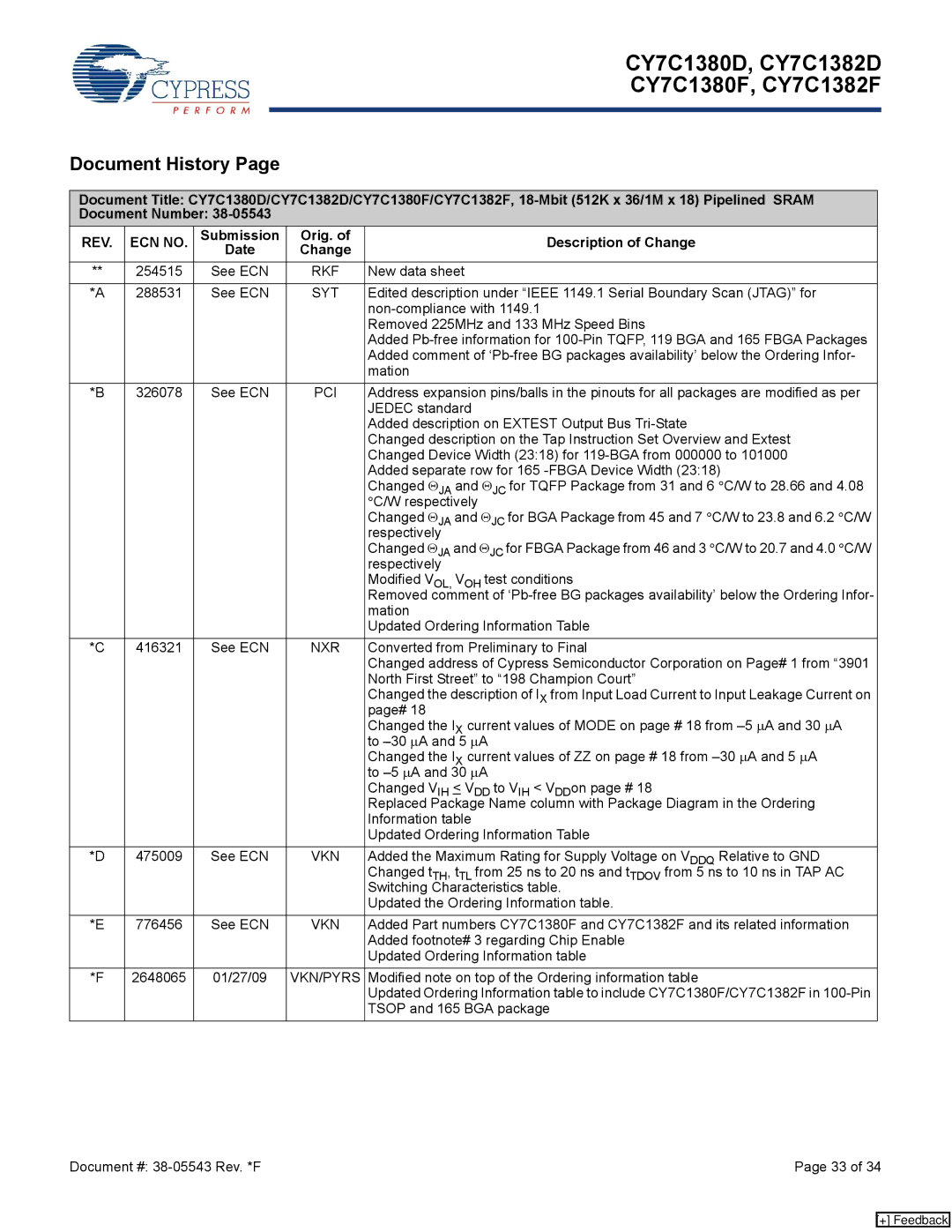
Document History Page
Document Title: CY7C1380D/CY7C1382D/CY7C1380F/CY7C1382F,
Document Number:
REV. | ECN NO. | Submission | Orig. of | Description of Change |
|
| Date | Change |
|
** | 254515 | See ECN | RKF | New data sheet |
|
|
|
|
|
*A | 288531 | See ECN | SYT | Edited description under “IEEE 1149.1 Serial Boundary Scan (JTAG)” for |
|
|
|
| |
|
|
|
| Removed 225MHz and 133 MHz Speed Bins |
|
|
|
| Added |
|
|
|
| Added comment of |
|
|
|
| mation |
*B | 326078 | See ECN | PCI | Address expansion pins/balls in the pinouts for all packages are modified as per |
|
|
|
| JEDEC standard |
|
|
|
| Added description on EXTEST Output Bus |
|
|
|
| Changed description on the Tap Instruction Set Overview and Extest |
|
|
|
| Changed Device Width (23:18) for |
|
|
|
| Added separate row for 165 |
|
|
|
| Changed ΘJA and ΘJC for TQFP Package from 31 and 6 °C/W to 28.66 and 4.08 |
|
|
|
| °C/W respectively |
|
|
|
| Changed ΘJA and ΘJC for BGA Package from 45 and 7 °C/W to 23.8 and 6.2 °C/W |
|
|
|
| respectively |
|
|
|
| Changed ΘJA and ΘJC for FBGA Package from 46 and 3 °C/W to 20.7 and 4.0 °C/W |
|
|
|
| respectively |
|
|
|
| Modified VOL, VOH test conditions |
|
|
|
| Removed comment of |
|
|
|
| mation |
|
|
|
| Updated Ordering Information Table |
*C | 416321 | See ECN | NXR | Converted from Preliminary to Final |
|
|
|
| Changed address of Cypress Semiconductor Corporation on Page# 1 from “3901 |
|
|
|
| North First Street” to “198 Champion Court” |
|
|
|
| Changed the description of IX from Input Load Current to Input Leakage Current on |
|
|
|
| page# 18 |
|
|
|
| Changed the IX current values of MODE on page # 18 from |
|
|
|
| to |
|
|
|
| Changed the IX current values of ZZ on page # 18 from |
|
|
|
| to |
|
|
|
| Changed VIH < VDD to VIH < VDDon page # 18 |
|
|
|
| Replaced Package Name column with Package Diagram in the Ordering |
|
|
|
| Information table |
|
|
|
| Updated Ordering Information Table |
*D | 475009 | See ECN | VKN | Added the Maximum Rating for Supply Voltage on VDDQ Relative to GND |
|
|
|
| Changed tTH, tTL from 25 ns to 20 ns and tTDOV from 5 ns to 10 ns in TAP AC |
|
|
|
| Switching Characteristics table. |
|
|
|
| Updated the Ordering Information table. |
*E | 776456 | See ECN | VKN | Added Part numbers CY7C1380F and CY7C1382F and its related information |
|
|
|
| Added footnote# 3 regarding Chip Enable |
|
|
|
| Updated Ordering Information table |
*F | 2648065 | 01/27/09 | VKN/PYRS | Modified note on top of the Ordering information table |
|
|
|
| Updated Ordering Information table to include CY7C1380F/CY7C1382F in |
|
|
|
| TSOP and 165 BGA package |
Document #: | Page 33 of 34 |
[+] Feedback