|
|
|
|
|
| CY7C1380C | |
|
|
|
|
|
| CY7C1382C | |
|
|
|
|
|
|
| |
|
|
|
|
|
|
|
|
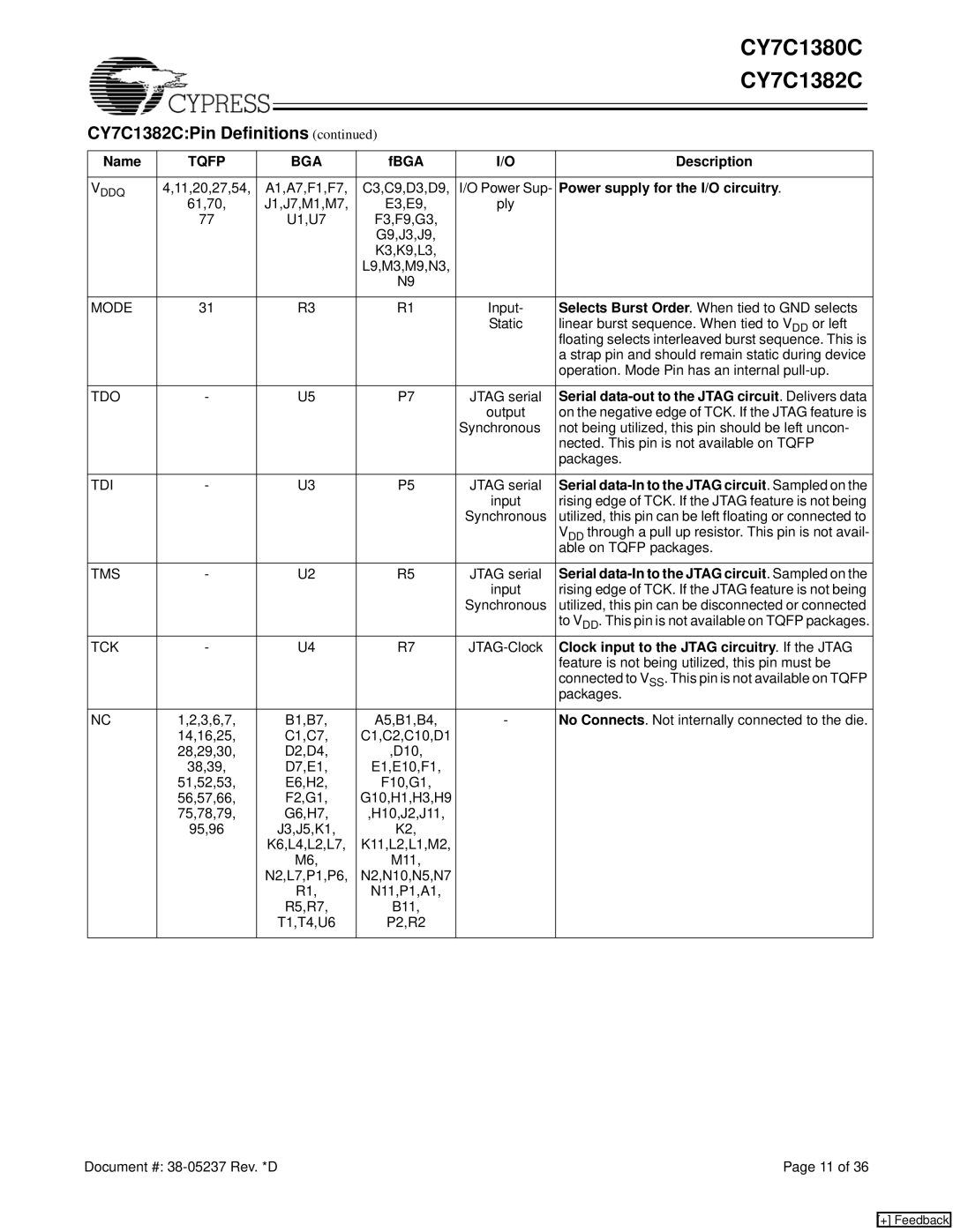
CY7C1382C:Pin Definitions (continued) |
|
|
| ||||
|
|
|
|
|
|
| |
Name | TQFP |
| BGA | fBGA | I/O | Description | |
|
|
|
|
|
| ||
VDDQ | 4,11,20,27,54, | A1,A7,F1,F7, | C3,C9,D3,D9, | I/O Power Sup- | Power supply for the I/O circuitry. | ||
| 61,70, | J1,J7,M1,M7, | E3,E9, | ply |
|
| |
| 77 |
| U1,U7 | F3,F9,G3, |
|
|
|
|
|
|
| G9,J3,J9, |
|
|
|
|
|
|
| K3,K9,L3, |
|
|
|
|
|
|
| L9,M3,M9,N3, |
|
|
|
|
|
|
| N9 |
|
|
|
|
|
|
|
|
|
| |
MODE | 31 |
| R3 | R1 | Input- | Selects Burst Order. When tied to GND selects | |
|
|
|
|
| Static | linear burst sequence. When tied to VDD or left | |
|
|
|
|
|
| floating selects interleaved burst sequence. This is | |
|
|
|
|
|
| a strap pin and should remain static during device | |
|
|
|
|
|
| operation. Mode Pin has an internal | |
|
|
|
|
|
|
| |
TDO | - |
| U5 | P7 | JTAG serial | Serial | |
|
|
|
|
| output | on the negative edge of TCK. If the JTAG feature is | |
|
|
|
|
| Synchronous | not being utilized, this pin should be left uncon- | |
|
|
|
|
|
| nected. This pin is not available on TQFP | |
|
|
|
|
|
| packages. | |
|
|
|
|
|
|
| |
TDI | - |
| U3 | P5 | JTAG serial | Serial | |
|
|
|
|
| input | rising edge of TCK. If the JTAG feature is not being | |
|
|
|
|
| Synchronous | utilized, this pin can be left floating or connected to | |
|
|
|
|
|
| VDD through a pull up resistor. This pin is not avail- | |
|
|
|
|
|
| able on TQFP packages. | |
|
|
|
|
|
|
| |
TMS | - |
| U2 | R5 | JTAG serial | Serial | |
|
|
|
|
| input | rising edge of TCK. If the JTAG feature is not being | |
|
|
|
|
| Synchronous | utilized, this pin can be disconnected or connected | |
|
|
|
|
|
| to VDD. This pin is not available on TQFP packages. | |
TCK | - |
| U4 | R7 | Clock input to the JTAG circuitry. If the JTAG | ||
|
|
|
|
|
| feature is not being utilized, this pin must be | |
|
|
|
|
|
| connected to VSS. This pin is not available on TQFP | |
|
|
|
|
|
| packages. | |
|
|
|
|
|
|
| |
NC | 1,2,3,6,7, |
| B1,B7, | A5,B1,B4, | - | No Connects. Not internally connected to the die. | |
| 14,16,25, |
| C1,C7, | C1,C2,C10,D1 |
|
|
|
| 28,29,30, |
| D2,D4, | ,D10, |
|
|
|
| 38,39, |
| D7,E1, | E1,E10,F1, |
|
|
|
| 51,52,53, |
| E6,H2, | F10,G1, |
|
|
|
| 56,57,66, |
| F2,G1, | G10,H1,H3,H9 |
|
|
|
| 75,78,79, |
| G6,H7, | ,H10,J2,J11, |
|
|
|
| 95,96 |
| J3,J5,K1, | K2, |
|
|
|
|
| K6,L4,L2,L7, | K11,L2,L1,M2, |
|
|
| |
|
|
| M6, | M11, |
|
|
|
|
| N2,L7,P1,P6, | N2,N10,N5,N7 |
|
|
| |
|
|
| R1, | N11,P1,A1, |
|
|
|
|
|
| R5,R7, | B11, |
|
|
|
|
|
| T1,T4,U6 | P2,R2 |
|
|
|
|
|
|
|
|
|
|
|
Document #: | Page 11 of 36 |
[+] Feedback