|
|
|
|
|
|
|
|
|
|
|
|
|
|
|
|
|
| CY7C1380C |
|
|
|
|
|
|
|
|
|
|
|
|
|
|
|
|
|
|
| CY7C1382C |
|
|
|
|
|
|
|
|
|
|
|
|
|
|
|
|
|
|
|
| |
|
|
|
|
|
|
|
|
|
|
|
|
|
|
|
|
|
|
|
|
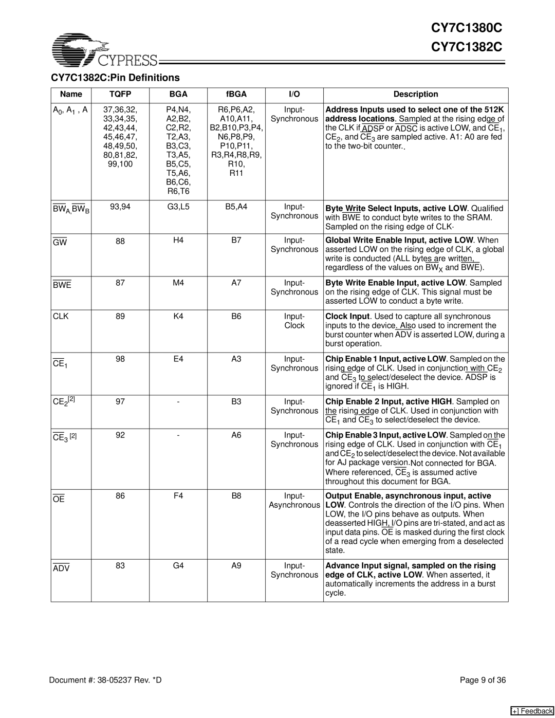
CY7C1382C:Pin Definitions |
|
|
|
|
|
|
|
| |||||||||||
|
|
|
|
|
|
|
|
|
|
| |||||||||
| Name | TQFP |
| BGA | fBGA | I/O |
|
| Description |
| |||||||||
|
|
|
|
|
|
|
|
| |||||||||||
| A0, A1 , A | 37,36,32, |
| P4,N4, | R6,P6,A2, | Input- | Address Inputs used to select one of the 512K |
| |||||||||||
|
|
|
|
|
|
|
|
| 33,34,35, |
| A2,B2, | A10,A11, | Synchronous | address locations. Sampled at the rising edge of |
| ||||
|
|
|
|
|
|
|
|
| 42,43,44, |
| C2,R2, | B2,B10,P3,P4, |
| the CLK if ADSP or ADSC is active LOW, and CE1, |
| ||||
|
|
|
|
|
|
|
|
| 45,46,47, |
| T2,A3, | N6,P8,P9, |
| CE2, and CE3 are sampled active. A1: A0 are fed |
| ||||
|
|
|
|
|
|
|
|
| 48,49,50, |
| B3,C3, | P10,P11, |
| to the |
| ||||
|
|
|
|
|
|
|
|
| 80,81,82, |
| T3,A5, | R3,R4,R8,R9, |
|
|
|
|
|
|
|
|
|
|
|
|
|
|
|
| 99,100 |
| B5,C5, | R10, |
|
|
|
|
|
|
|
|
|
|
|
|
|
|
|
|
|
| T5,A6, | R11 |
|
|
|
|
|
|
|
|
|
|
|
|
|
|
|
|
|
| B6,C6, |
|
|
|
|
|
|
|
|
|
|
|
|
|
|
|
|
|
|
| R6,T6 |
|
|
|
|
|
|
|
|
|
|
|
|
|
|
|
|
|
|
|
|
| |||||||
|
|
| A, |
| B | 93,94 |
| G3,L5 | B5,A4 | Input- | Byte Write Select Inputs, active LOW. Qualified |
| |||||||
| BW | BW |
| ||||||||||||||||
|
|
|
|
|
|
|
|
|
|
|
|
| Synchronous | with | BWE | to conduct byte writes to the SRAM. |
| ||
|
|
|
|
|
|
|
|
|
|
|
|
|
| Sampled on the rising edge of CLK. |
| ||||
|
|
|
|
|
|
| 88 |
| H4 | B7 | Input- | Global Write Enable Input, active LOW. When |
| ||||||
| GW |
| |||||||||||||||||
|
|
|
|
|
|
|
|
|
|
|
|
| Synchronous | asserted LOW on the rising edge of CLK, a global |
| ||||
|
|
|
|
|
|
|
|
|
|
|
|
|
| write is conducted (ALL bytes are written, |
| ||||
|
|
|
|
|
|
|
|
|
|
|
|
|
| regardless of the values on BWX and BWE). |
| ||||
|
|
|
|
|
|
| 87 |
| M4 | A7 | Input- | Byte Write Enable Input, active LOW. Sampled |
| ||||||
| BWE |
| |||||||||||||||||
|
|
|
|
|
|
|
|
|
|
|
|
| Synchronous | on the rising edge of CLK. This signal must be |
| ||||
|
|
|
|
|
|
|
|
|
|
|
|
|
| asserted LOW to conduct a byte write. |
| ||||
|
|
|
|
|
|
|
|
| |||||||||||
| CLK | 89 |
| K4 | B6 | Input- | Clock Input. Used to capture all synchronous |
| |||||||||||
|
|
|
|
|
|
|
|
|
|
|
|
| Clock | inputs to the device. Also used to increment the |
| ||||
|
|
|
|
|
|
|
|
|
|
|
|
|
| burst counter when | ADV | is asserted LOW, during a |
| ||
|
|
|
|
|
|
|
|
|
|
|
|
|
| burst operation. |
| ||||
|
|
|
|
|
|
|
|
|
|
|
|
|
|
|
| ||||
|
|
|
|
|
|
|
|
| 98 |
| E4 | A3 | Input- | Chip Enable 1 Input, active LOW. Sampled on the |
| ||||
| CE1 |
| |||||||||||||||||
|
|
|
|
| Synchronous | rising edge of CLK. Used in conjunction with CE2 |
| ||||||||||||
|
|
|
|
|
|
|
|
|
|
|
|
|
| and CE3 to select/deselect the device. ADSP is |
| ||||
|
|
|
|
|
|
|
|
|
|
|
|
|
| ignored if CE1 is HIGH. |
| ||||
| CE2[2] | 97 |
| - | B3 | Input- | Chip Enable 2 Input, active HIGH. Sampled on |
| |||||||||||
|
|
|
|
|
|
|
|
|
|
|
|
| Synchronous | the rising edge of CLK. Used in conjunction with |
| ||||
|
|
|
|
|
|
|
|
|
|
|
|
|
| CE1 and CE3 to select/deselect the device. |
| ||||
|
| 3 [2] | 92 |
| - | A6 | Input- | Chip Enable 3 Input, active LOW. Sampled on the |
| ||||||||||
| CE |
| |||||||||||||||||
|
|
|
|
|
|
|
|
|
|
|
|
| Synchronous | rising edge of CLK. Used in conjunction with CE1 |
| ||||
|
|
|
|
|
|
|
|
|
|
|
|
|
| and CE2 to select/deselect the device. Not available |
| ||||
|
|
|
|
|
|
|
|
|
|
|
|
|
| for AJ package version.Not connected for BGA. |
| ||||
|
|
|
|
|
|
|
|
|
|
|
|
|
| Where referenced, CE3 is assumed active |
| ||||
|
|
|
|
|
|
|
|
|
|
|
|
|
| throughout this document for BGA. |
| ||||
|
|
|
|
|
|
|
|
|
|
|
|
|
|
|
| ||||
|
|
|
|
|
|
|
|
| 86 |
| F4 | B8 | Input- | Output Enable, asynchronous input, active |
| ||||
| OE |
| |||||||||||||||||
|
|
|
|
| Asynchronous | LOW. Controls the direction of the I/O pins. When |
| ||||||||||||
|
|
|
|
|
|
|
|
|
|
|
|
|
| ||||||
|
|
|
|
|
|
|
|
|
|
|
|
|
| LOW, the I/O pins behave as outputs. When |
| ||||
|
|
|
|
|
|
|
|
|
|
|
|
|
| deasserted HIGH, I/O pins are |
| ||||
|
|
|
|
|
|
|
|
|
|
|
|
|
| input data pins. OE is masked during the first clock |
| ||||
|
|
|
|
|
|
|
|
|
|
|
|
|
| of a read cycle when emerging from a deselected |
| ||||
|
|
|
|
|
|
|
|
|
|
|
|
|
| state. |
| ||||
|
|
|
|
|
|
|
|
|
| ||||||||||
|
|
|
|
|
| 83 |
| G4 | A9 | Input- | Advance Input signal, sampled on the rising |
| |||||||
| ADV |
| |||||||||||||||||
|
|
|
|
|
|
|
|
|
|
|
|
| Synchronous | edge of CLK, active LOW. When asserted, it |
| ||||
|
|
|
|
|
|
|
|
|
|
|
|
|
| automatically increments the address in a burst |
| ||||
|
|
|
|
|
|
|
|
|
|
|
|
|
| cycle. |
| ||||
|
|
|
|
|
|
|
|
|
|
|
|
|
|
|
|
|
|
|
|
Document #: | Page 9 of 36 |
[+] Feedback