CLK
tCH
tADS tADH
ADSP
ADSC
tAS tAH
tCL
tADS tADH
ADDRESS
GW, BWE, BWx
CE
ADV
OE
Data Out (Q)
A1 | A2 | A3 |
tWES | tWEH | Burst continued with |
new base address | ||
tCES tCEH |
| Deselect |
| cycle |
tADVS tADVH
![]() ADV suspends burst.
ADV suspends burst.
|
| tOEV | tCO |
|
|
|
|
|
| tOEHZ | tOELZ | tDOH |
|
|
|
| tCHZ |
| tCLZ |
|
|
|
|
|
|
|
Q(A1) |
| Q(A2) | Q(A2 + 1) | Q(A2 + 2) | Q(A2 + 3) | Q(A2) | Q(A2 + 1) | |
| tCO |
|
|
|
|
|
|
|
|
|
|
|
|
|
| Burst wraps around | |
|
|
|
|
|
|
| to its initial state | |
| Single READ |
|
|
| BURST READ |
|
|
|
|
|
| DON’T CARE |
| UNDEFINED |
|
|
|
Notes:
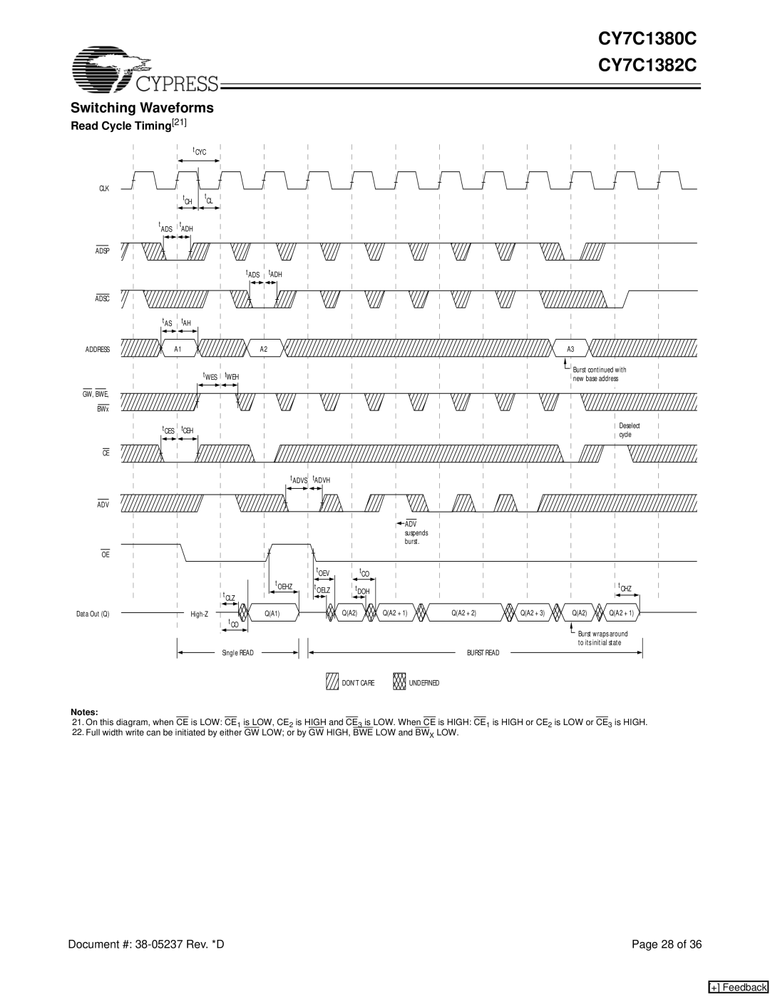
21.On this diagram, when CE is LOW: CE1 is LOW, CE2 is HIGH and CE3 is LOW. When CE is HIGH: CE1 is HIGH or CE2 is LOW or CE3 is HIGH.
22.Full width write can be initiated by either GW LOW; or by GW HIGH, BWE LOW and BWX LOW.
Document #: | Page 28 of 36 |
[+] Feedback