CY7C1380C
CY7C1382C
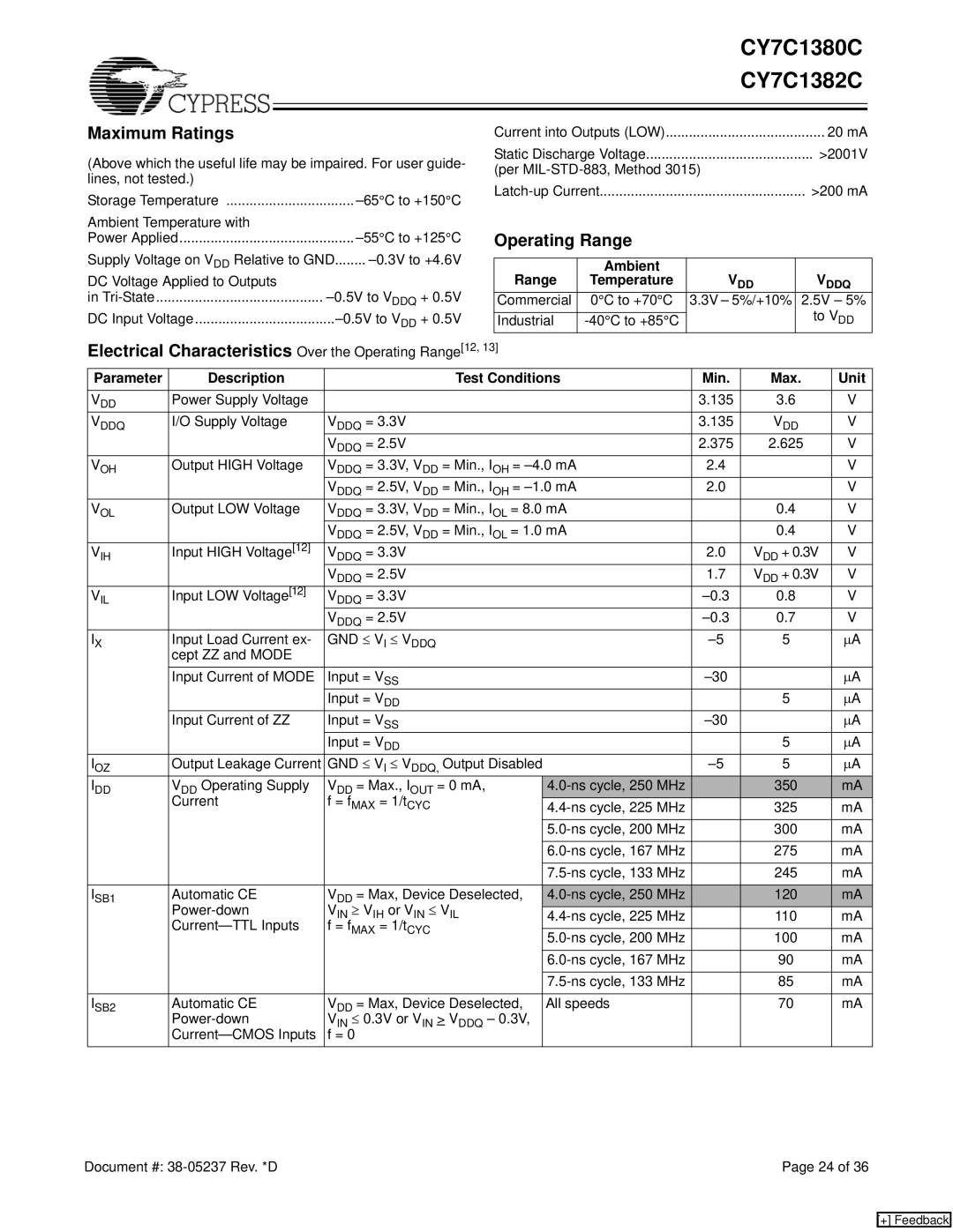
Maximum Ratings
(Above which the useful life may be impaired. For user guide- lines, not tested.)
Storage Temperature | ||
Ambient Temperature with |
|
|
Power Applied | ||
Supply Voltage on VDD Relative to GND | ........ | |
DC Voltage Applied to Outputs |
|
|
in | ||
DC Input Voltage | ||
Current into Outputs (LOW) | 20 mA |
Static Discharge Voltage | >2001V |
(per |
|
>200 mA |
Operating Range
| Ambient |
|
|
Range | Temperature | VDD | VDDQ |
Commercial | 0°C to +70°C | 3.3V – 5%/+10% | 2.5V – 5% |
|
|
| to VDD |
Industrial |
|
Electrical Characteristics Over the Operating Range[12, 13]
Parameter | Description | Test Conditions | Min. | Max. | Unit | |
VDD | Power Supply Voltage |
|
| 3.135 | 3.6 | V |
VDDQ | I/O Supply Voltage | VDDQ = 3.3V |
| 3.135 | VDD | V |
|
| VDDQ = 2.5V |
| 2.375 | 2.625 | V |
VOH | Output HIGH Voltage | VDDQ = 3.3V, VDD = Min., IOH = | 2.4 |
| V | |
|
| VDDQ = 2.5V, VDD = Min., IOH = | 2.0 |
| V | |
VOL | Output LOW Voltage | VDDQ = 3.3V, VDD = Min., IOL = 8.0 mA |
| 0.4 | V | |
|
| VDDQ = 2.5V, VDD = Min., IOL = 1.0 mA |
| 0.4 | V | |
VIH | Input HIGH Voltage[12] | VDDQ = 3.3V |
| 2.0 | VDD + 0.3V | V |
|
| VDDQ = 2.5V |
| 1.7 | VDD + 0.3V | V |
VIL | Input LOW Voltage[12] | VDDQ = 3.3V |
| 0.8 | V | |
|
| VDDQ = 2.5V |
| 0.7 | V | |
IX | Input Load Current ex- | GND ≤ VI ≤ VDDQ |
| 5 | ∝A | |
| cept ZZ and MODE |
|
|
|
|
|
| Input Current of MODE | Input = VSS |
|
| ∝A | |
|
| Input = VDD |
|
| 5 | ∝A |
| Input Current of ZZ | Input = VSS |
|
| ∝A | |
|
| Input = VDD |
|
| 5 | ∝A |
IOZ | Output Leakage Current | GND ≤ VI ≤ VDDQ, Output Disabled |
| 5 | ∝A | |
IDD | VDD Operating Supply | VDD = Max., IOUT = 0 mA, |
| 350 | mA | |
| Current | f = fMAX = 1/tCYC |
| 325 | mA | |
|
|
|
| 300 | mA | |
|
|
|
|
|
|
|
|
|
|
| 275 | mA | |
|
|
|
|
|
|
|
|
|
|
| 245 | mA | |
|
|
|
|
|
|
|
ISB1 | Automatic CE | VDD = Max, Device Deselected, |
| 120 | mA | |
| VIN ≥ VIH or VIN ≤ VIL |
| 110 | mA | ||
| f = fMAX = 1/tCYC |
|
|
|
| |
|
| 100 | mA | |||
|
|
|
| |||
|
|
|
|
|
|
|
|
|
|
| 90 | mA | |
|
|
|
|
|
|
|
|
|
|
| 85 | mA | |
|
|
|
|
|
|
|
ISB2 | Automatic CE | VDD = Max, Device Deselected, | All speeds |
| 70 | mA |
| VIN ≤ 0.3V or VIN > VDDQ – 0.3V, |
|
|
|
| |
| f = 0 |
|
|
|
| |
Document #: | Page 24 of 36 |
[+] Feedback