CY7C68053

9.13.4Sequence Diagram of a Single and Burst Asynchronous Write

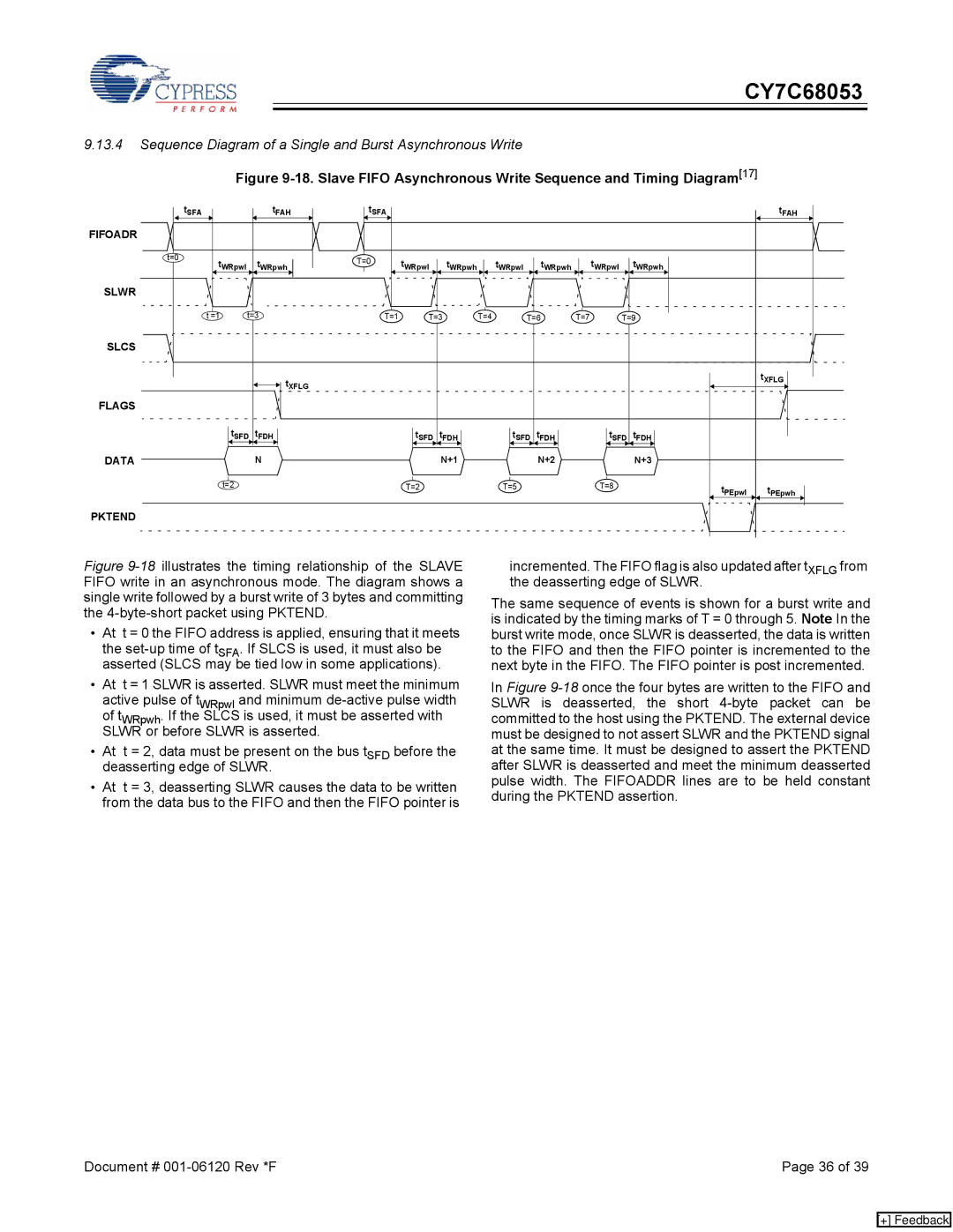
Figure 9-18. Slave FIFO Asynchronous Write Sequence and Timing Diagram[17]


tSFA


tFAH

tSFA


tFAH

FIFOADR


t=0

tWRpwl

tWRpwh

T=0

tWRpwl

tWRpwh


tWRpwl

tWRpwh

tWRpwl


tWRpwh


SLWR


t =1

t=3

T=1

T=3

T=4

T=6

T=7

T=9


SLCS


tXFLG


tXFLG


FLAGS


tSFD

tFDH


tSFD

tFDH


tSFD

tFDH

tSFD

tFDH


DATA


N


N+1


N+2


N+3


t=2


T=2


T=5


T=8


tPEpwl

tPEpwh


PKTEND


Figure 9-18illustrates the timing relationship of the SLAVE FIFO write in an asynchronous mode. The diagram shows a single write followed by a burst write of 3 bytes and committing the 4-byte-short packet using PKTEND.

At t = 0 the FIFO address is applied, ensuring that it meets the set-up time of tSFA. If SLCS is used, it must also be asserted (SLCS may be tied low in some applications).

At t = 1 SLWR is asserted. SLWR must meet the minimum active pulse of tWRpwl and minimum de-active pulse width of tWRpwh. If the SLCS is used, it must be asserted with SLWR or before SLWR is asserted.

At t = 2, data must be present on the bus tSFD before the deasserting edge of SLWR.

At t = 3, deasserting SLWR causes the data to be written from the data bus to the FIFO and then the FIFO pointer is

incremented. The FIFO flag is also updated after tXFLG from the deasserting edge of SLWR.

The same sequence of events is shown for a burst write and is indicated by the timing marks of T = 0 through 5. Note In the burst write mode, once SLWR is deasserted, the data is written to the FIFO and then the FIFO pointer is incremented to the next byte in the FIFO. The FIFO pointer is post incremented.

In Figure 9-18once the four bytes are written to the FIFO and SLWR is deasserted, the short 4-byte packet can be committed to the host using the PKTEND. The external device must be designed to not assert SLWR and the PKTEND signal at the same time. It must be designed to assert the PKTEND after SLWR is deasserted and meet the minimum deasserted pulse width. The FIFOADDR lines are to be held constant during the PKTEND assertion.

Document # 001-06120 Rev *F

Page 36 of 39

[+] Feedback

Page 36
Image 36
Cypress CY7C68053 manual Sequence Diagram of a Single and Burst Asynchronous Write

CY7C68053 specifications

The Cypress CY7C68053 is a versatile USB microcontroller known for its strong performance and rich feature set, catering to a wide range of applications requiring USB connectivity. Part of the Cypress family of USB products, this microcontroller combines the convenience of USB interfacing with powerful embedded processing capabilities.

At its core, the CY7C68053 is built on an 8051 microcontroller architecture, enabling efficient data handling and control operations. It operates at speeds of up to 48 MHz, providing ample processing power for complex applications. The device features an integrated USB 2.0 full-speed controller, which allows for high-speed data transfer rates of up to 12 Mbps. This makes it ideal for applications such as data transfer, communication devices, and real-time processing tasks.

One of the standout features of the CY7C68053 is its flexible pin configuration. It supports a variety of operating modes, including peripheral mode, host mode, and a combination of both, allowing it to cater to diverse application requirements. Additionally, the device offers a large number of GPIO pins that can be used for various control and communication tasks. This flexibility ensures that developers can tailor the hardware to meet the specific needs of their application.

In terms of development, the CY7C68053 is backed by a robust set of software development tools from Cypress. The EZ-USB development kit provides a comprehensive platform for firmware development, testing, and debugging. This kit includes libraries, example projects, and a user-friendly integrated development environment (IDE), streamlining the development process for engineers.

The CY7C68053 is also equipped with an extensive memory system, featuring 32 kB of in-system programmable Flash memory, 2 kB of SRAM, and 128 bytes of EEPROM. This memory capacity allows for the storage of complex firmware and user data, enhancing the device's versatility.

Moreover, the CY7C68053 is designed with low power consumption in mind. It includes power management features that allow it to operate efficiently, making it suitable for battery-operated devices.

In summary, the Cypress CY7C68053 stands out as a powerful USB microcontroller that combines high-speed processing, flexible configurations, and robust software support. Its features make it an excellent choice for developers looking to create innovative USB-enabled products across various applications.