CY8C24123A

CY8C24223A, CY8C24423A

Table 9. Register Map Bank 0 Table: User Space (continued)

Name

Addr

Access

Name

Addr

Access

Name

Addr

Access

Name

Addr

Access

(0,Hex)

(0,Hex)

(0,Hex)

(0,Hex)


3E


7E


BE


CPU_SCR1

FE

#


3F


7F


BF


CPU_SCR0

FF

#

Blank fields are

Reserved and must not be accessed.


# Access is bit specific.


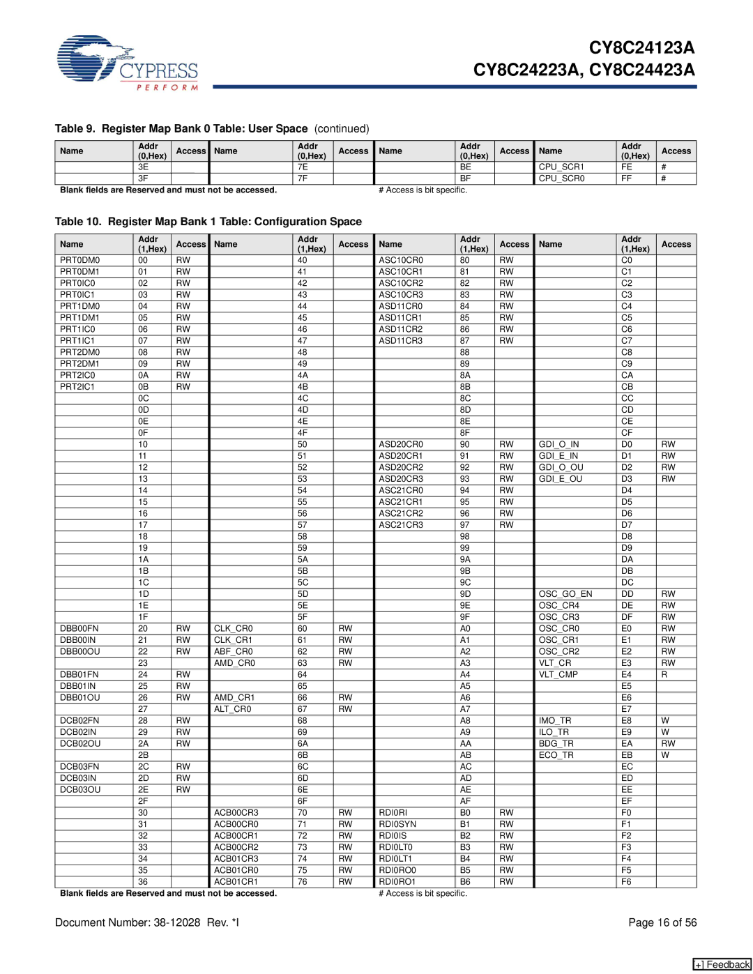
Table 10. Register Map Bank 1 Table: Configuration Space

Name

Addr

Access

Name

Addr

Access

Name

Addr

Access

Name

Addr

Access

(1,Hex)

(1,Hex)

(1,Hex)

(1,Hex)

PRT0DM0

00

RW


40


ASC10CR0

80

RW


C0


PRT0DM1

01

RW


41


ASC10CR1

81

RW


C1


PRT0IC0

02

RW


42


ASC10CR2

82

RW


C2


PRT0IC1

03

RW


43


ASC10CR3

83

RW


C3


PRT1DM0

04

RW


44


ASD11CR0

84

RW


C4


PRT1DM1

05

RW


45


ASD11CR1

85

RW


C5


PRT1IC0

06

RW


46


ASD11CR2

86

RW


C6


PRT1IC1

07

RW


47


ASD11CR3

87

RW


C7


PRT2DM0

08

RW


48


88


C8


PRT2DM1

09

RW


49


89


C9


PRT2IC0

0A

RW


4A


8A


CA


PRT2IC1

0B

RW


4B


8B


CB


0C


4C


8C


CC


0D


4D


8D


CD


0E


4E


8E


CE


0F


4F


8F


CF


10


50


ASD20CR0

90

RW

GDI_O_IN

D0

RW


11


51


ASD20CR1

91

RW

GDI_E_IN

D1

RW


12


52


ASD20CR2

92

RW

GDI_O_OU

D2

RW


13


53


ASD20CR3

93

RW

GDI_E_OU

D3

RW


14


54


ASC21CR0

94

RW


D4


15


55


ASC21CR1

95

RW


D5


16


56


ASC21CR2

96

RW


D6


17


57


ASC21CR3

97

RW


D7


18


58


98


D8


19


59


99


D9


1A


5A


9A


DA


1B


5B


9B


DB


1C


5C


9C


DC


1D


5D


9D


OSC_GO_EN

DD

RW


1E


5E


9E


OSC_CR4

DE

RW


1F


5F


9F


OSC_CR3

DF

RW

DBB00FN

20

RW

CLK_CR0

60

RW


A0


OSC_CR0

E0

RW

DBB00IN

21

RW

CLK_CR1

61

RW


A1


OSC_CR1

E1

RW

DBB00OU

22

RW

ABF_CR0

62

RW


A2


OSC_CR2

E2

RW


23


AMD_CR0

63

RW


A3


VLT_CR

E3

RW

DBB01FN

24

RW


64


A4


VLT_CMP

E4

R

DBB01IN

25

RW


65


A5


E5


DBB01OU

26

RW

AMD_CR1

66

RW


A6


E6


27


ALT_CR0

67

RW


A7


E7


DCB02FN

28

RW


68


A8


IMO_TR

E8

W

DCB02IN

29

RW


69


A9


ILO_TR

E9

W

DCB02OU

2A

RW


6A


AA


BDG_TR

EA

RW


2B


6B


AB


ECO_TR

EB

W

DCB03FN

2C

RW


6C


AC


EC


DCB03IN

2D

RW


6D


AD


ED


DCB03OU

2E

RW


6E


AE


EE


2F


6F


AF


EF


30


ACB00CR3

70

RW

RDI0RI

B0

RW


F0


31


ACB00CR0

71

RW

RDI0SYN

B1

RW


F1


32


ACB00CR1

72

RW

RDI0IS

B2

RW


F2


33


ACB00CR2

73

RW

RDI0LT0

B3

RW


F3


34


ACB01CR3

74

RW

RDI0LT1

B4

RW


F4


35


ACB01CR0

75

RW

RDI0RO0

B5

RW


F5


36


ACB01CR1

76

RW

RDI0RO1

B6

RW


F6


Blank fields are

Reserved and must not be accessed.


# Access is bit specific.


Document Number: 38-12028 Rev. *I


Page 16 of 56

[+] Feedback

Page 16
Image 16
Cypress CY8C24123A manual Register Map Bank 1 Table Configuration Space

CY8C24123A specifications

The Cypress CY8C24123A is a prominent member of the PSoC (Programmable System-on-Chip) family, which integrates a microcontroller with programmable analog and digital components on a single chip. Designed for low-power applications, the CY8C24123A offers a compelling mix of features and technologies that make it a popular choice for embedded system developers.

One of the standout features of the CY8C24123A is its low power consumption, which allows it to extend battery life in portable applications. It operates at a voltage range of 1.71V to 5.5V, making it versatile for various power supply options. This device is equipped with a 24 MHz CPU that efficiently executes tasks while keeping energy usage minimal.

The chip boasts a rich set of programmable peripherals, including analog components such as operational amplifiers, comparators, and DACs, enabling designers to create custom signal processing pathways. These features are complemented by a variety of digital peripherals, like timers, UART, I2C, and SPI interfaces, which facilitate communication with other devices and microcontrollers. The integration of these components reduces the need for external components, leading to a more compact design and lower overall system costs.

Moreover, the CY8C24123A includes Flash memory (up to 2 KB) and SRAM (256 bytes), providing ample storage for application code and data. This Flash memory is reprogrammable, enabling developers to update their applications easily without needing to replace the chip.

Another defining characteristic of the CY8C24123A is its programmability. The device can be configured and programmed using the Cypress PSoC Designer software, which allows developers to design and simulate their applications in a user-friendly environment. The combination of hardware-based flexibility and software configuration provides a robust platform for creating custom solutions tailored to specific application requirements.

Overall, the Cypress CY8C24123A stands out for its balance of performance, programmability, and power efficiency. Its integration of programmable analog and digital blocks makes it suitable for a wide range of applications, including industrial control, consumer electronics, and automotive systems. The ability to customize the chip's functionality further boosts its appeal, making it an excellent choice for developers seeking a versatile and efficient solution for their embedded projects.