| FIGURES |
|
|
| page |
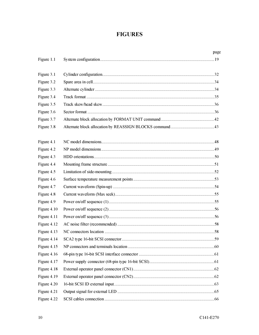
Figure 1.1 | System configuration | 19 |
Figure 3.1 | Cylinder configuration | 32 |
Figure 3.2 | Spare area in cell | 34 |
Figure 3.3 | Alternate cylinder | 34 |
Figure 3.4 | Track format | 35 |
Figure 3.5 | Track skew/head skew | 36 |
Figure 3.6 | Sector format | 36 |
Figure 3.7 | Alternate block allocation by FORMAT UNIT command | 42 |
Figure 3.8 | Alternate block allocation by REASSIGN BLOCKS command | 43 |
Figure 4.1 | NC model dimensions | 48 |
Figure 4.2 | NP model dimensions | 49 |
Figure 4.3 | HDD orientations | 50 |
Figure 4.4 | Mounting frame structure | 51 |
Figure 4.5 | Limitation of | 52 |
Figure 4.6 | Surface temperature measurement points | 53 |
Figure 4.7 | Current waveform | 54 |
Figure 4.8 | Current waveform (Max seek) | 55 |
Figure 4.9 | Power on/off sequence (1) | 55 |
Figure 4.10 | Power on/off sequence (2) | 56 |
Figure 4.11 | Power on/off sequence (3) | 56 |
Figure 4.12 | AC noise filter (recommended) | 58 |
Figure 4.13 | NC connectors location | 58 |
Figure 4.14 | SCA2 type | 59 |
Figure 4.15 | NP connectors and terminals location | 60 |
Figure 4.16 | 61 | |
Figure 4.17 | Power supply connector | 61 |
Figure 4.18 | External operator panel connector (CN1) | 62 |
Figure 4.19 | External operator panel connector (CN2) | 62 |
Figure 4.20 | 63 | |
Figure 4.21 | Output signal for external LED | 65 |
Figure 4.22 | SCSI cables connection | 66 |
10 |
