Manuals
/
Fujitsu
/
Computer Equipment
/
Computer Drive
Fujitsu
MCM3130AP, MCM3064AP
manual
Ultra DMA data out transfer device stop timing
Models:
MCM3130AP
MCM3064AP
1
163
202
202
Download
202 pages
27.76 Kb
160
161
162
163
164
165
166
167
Specs
Install
Error codes
Signal Description
Error rate
Standby timer
Dimension
Maintenance
Configuration
Reset response
Page 163
Image 163
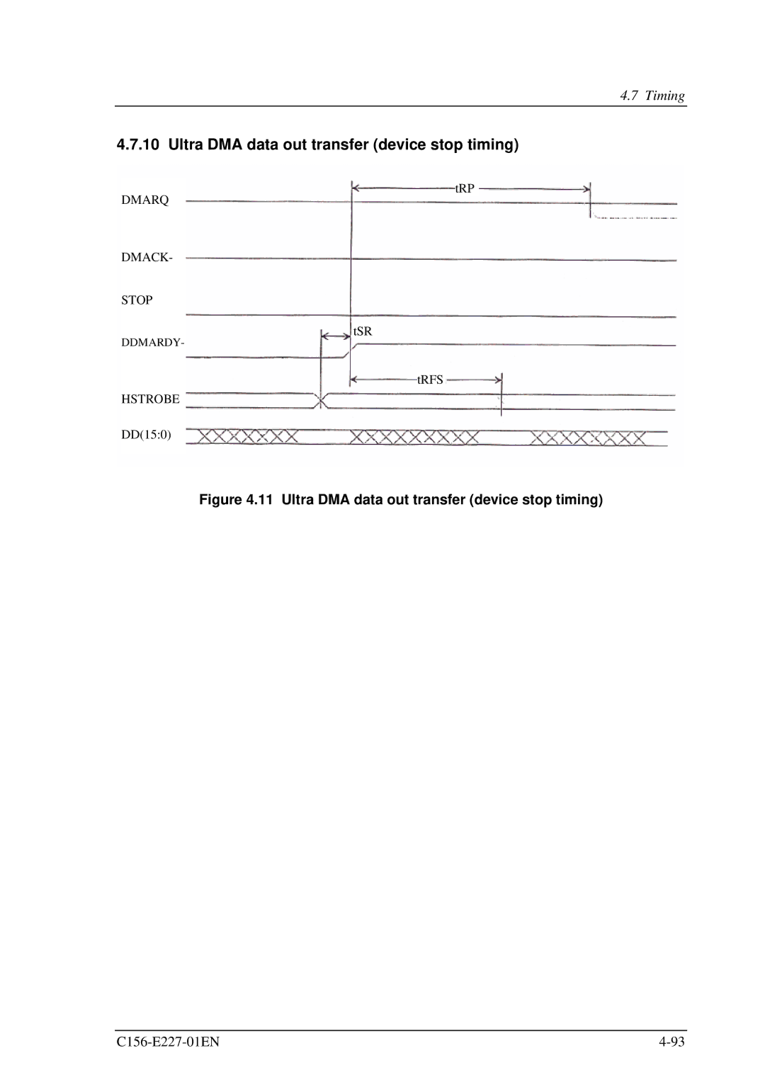
4.7 Timing
4.7.10 Ultra DMA data out transfer (device stop timing)
tRP
DMARQ
DMACK-
STOP
tSR
DDMARDY-
tRFS
HSTROBE
DD(15:0)
Figure 4.11 Ultra DMA data out transfer (device stop timing)
C156-E227-01EN
4-93
Page 162
Page 164
Page 163
Image 163
Page 162
Page 164
Contents
MCM3064AP, MCM3130AP
Handling of This Manual
For Safe Operation
Revision History
This page is intentionally left blank
Overview of Manual
Preface
Glossary
Preface
Acronyms and Abbreviations
Conventions for Alert Messages
This page is intentionally left blank
Important Alert Messages
Important Alert Items
Important Alert Items
C156-E227-01EN Vii
JTC1=
IEC=
Contents
Host Interface
Contents
Contents
Synchronize Cache command
Operation and Cleaning
Diagnostics and Maintenance
Ultra DMA data in transfer initialization timing
Illustrations
Tables
53 Drive Operation Mode Page default value
C156-E227-01EN Xvii
Xviii C156-E227-01EN
General Description
Features
Performance and Functions
General Description
Adaptability
Features
Reliability
Maintainability/operability
Interface
Features
Appearance
Configuration of Optical Disk Drive
Configuration of Optical Disk Drive
Configuration
Mechanical section
Control circuit section
Block diagram of the control circuit section
This page is intentionally left blank
Representative model names and order numbers
Specifications
Specifications of Optical Disk Drives
Catalog and order numbers
Specifications
Specifications of drives
Specifications 1
Specifications 2
Specifications of Optical Disk Drives
Environmental and power requirements 1
Environmental and power requirements
Environmental and power requirements 2
Error rate
Data loss
Mtbf =
Recommended optical disk cartridges
Specifications of Optical Disk Cartridges
Specifications of Optical Disk Cartridges
Recommended optical disk cartridges
Optical disk cartridge 1/2
Specifications of Optical Disk Cartridges
Disk specifications
Specifications of disk
Defect Management
Defect management schematic diagram
Defect Management
Example of alternate processing
Temperature measurement points
Installation Requirements
Environmental Requirements
Installation Requirements
Temperature requirements
Temperature requirements at measurement points
Temperatures at measuring points Reference
Temperature rise
Air cleanliness
Outer dimensions
Outer dimensions 1/2
Mounting Requirements
Outer dimensions 2/2
Outer dimensions 1/3
Outer dimensions 2/3
Outer dimensions 3/3
Installation directions
Installation direction
Center of gravity
Center of gravity
Mounting frame structure
Precautions on mounting
Service areas
Power Supply Requirements
Power Supply Requirements
Cable Connections
Drive connectors
+5 VDC Return GND
Cable connector specifications
Cable connector specifications
Cable Connections
Factory shipment settings
Jumper Settings
Drive connections
Jumper Settings
Mode settings
14 Cable selection mode setting
Precautions on Handling of Drive
Precautions on Handling of Drive
Device damage
Installation Requirements
16 Packing styles 1/2
16 Packing styles 2/2
Mounting of Drive
Mounting procedure
Mounting of Drive
Initial operation check
Post-installation Operation Check and Preparation for Use
Connection check
Post-installation Operation Check and Preparation for Use
Demounting of Drive
Host Interface
Pin Assignment
Connector pin assignments 1/2
Host Interface
Pin Assignment
Connector pin assignments 2/2
Signal description 1/2
Signal Description
Dior
Signal description 2/2
Signal Description
DA1 DA0
Interface Registers
1 I/O registers
I/O port functions and mapping
Data register
ATA Command register
Alternate Status register
Bit definitions of Alternate Status register
Bit definitions of Atapi Byte Count register
Drive Address register
Bit definitions of Drive Address register
Atapi Byte Count register
Bit definitions of Atapi Block Device Select register
Error register
Bit definitions of Error register
Atapi Block Device Select register
ATA Sector Count register
ATA Features register
Atapi Features register
10 Bit definitions of Atapi Features register
13 Bit definitions of Atapi Status register
12 I/O and C/D
Sector Number register
Atapi Status register
Host Interface
Various Processes
Reset response
Various Processes
Automatic alternate sector assignment function
Defect sector management
14 Alternate sector assignment criteria
Data error detection criteria
Data buffer
Cache function
Read cache
MO write cache
Media status notification function
Power management function
Idle mode
Power mode
Active mode
Pre-idle mode
Sleep mode
Standby mode
Standby timer
Power mode transition
16 LED indications
LED Indications
ATA Commands
ATA Commands
17 Command codes and parameters
Identify Packet Device A1h
19 Device parameter information 1/5
19 Device parameter information 2/5
19 Device parameter information 3/5
19 Device parameter information 4/5
19 Device parameter information 5/5
Packet A0h
20 Packet command
21 Device Reset command
Device Reset 08h
23 Power mode indication
Check Power Mode E5h
When device 1 is connected
Execute Device Diagnostic 90h
GET Media Status DAh
26 GET Media Status command
25 Self-diagnosis detailed code
28 Idle Immediate command
27 Error register
Idle Immediate 95h/E1h
NOP 00h
Service A2h
29 NOP command
30 Service command
31 SET Features command
SET Features EFh
DRV
32 FR register setting value
33 Transfer setting values in the SC register
34 Cylinder High register
Sleep 99h/E6h
35 Sleep command
Standby Immediate 94h-E0h
Packet Commands
Packet Commands
37 Packet command codes and parameters
38 Erase command
Erase command
Logical Unit Number
39 Format Unit command
Format Unit command
40 Format Unit parameter list
43 Inquiry command
Inquiry command
Format Descriptor
RMB
44 Inquiry data
45 Mode Select command
Mode Select command
46 Mode parameters
48 Mode parameter header
47 Mode parameter list
49 Block descriptor
50 Page Descriptor
Drive Operation Mode
SLM
DCR
52 Drive Operation Mode Page variable
Read-Write error recovery
PER
55 Changeable values in the read-write recovery
Flexible disk
56 Default values for the read-write recovery
58 Changeable values in flexible disk
59 Default values in flexible disk
WCE
Caching 60 Caching
61 Changeable values in the caching
Tlun
64 Removable Block Access Capabilities variable
Sflp
SML
Timer & Protect 66 Timer & Protect
65 Removable Block Access Capabilities Page default value
Disp
67 Inactivity Timer Multiplier values
68 Timer & Protect Page variable
Mode Sense 10 command
70 Mode Sense 10 command
73 Mode Parameter Header
72 Mode Parameter List
71 Page Control field
74 Page Descriptor
78 Mode parameter header
Mode Sense 6 command
76 Mode Sense 6 command
77 Mode parameter list
START/STOP Unit Sense KEY
PREVENT/ALLOW Medium Removal command
79 PREVENT/ALLOW Medium Removal command
80 Response to Prevent/Allow/Eject
82 Read command
Read 10 command
Read 12 command
81 Read 10 command
85 Read Capacity data PMI=1, MO media, from medium
Read Capacity command
83 Read Capacity command
84 Read Capacity data PMI=0
88 Read Format Capacities data format
Read Format Capacities command
87 Read Format Capacities command
86 Read Capacity data PMI=1, Prom medium
91 Descriptor code definition
Read Defect Data command
92 Read Defect Data command
90 Current/Maximum capacity descriptor
94 Defect List Header
93 Defect List Format
97 Receive Diagnostic Results command
Read Long command
Receive Diagnostic Results command
96 Read Long command
98 Request Sense command
Request Sense command
99 Request sense data
100 Error code
102 Logical block address format
101 Sense Key code
103 ASC/ASCQ list 1/2
104 Format Progress Indication Bytes
103 ASC/ASCQ list 2/2
106 Seek command
Send Diagnostic command
Seek command
105 Send Diagnostic command
107 START/STOP Unit command
START/STOP Unit command
108 START/STOP/EJECT processing
110 Test Unit Ready command
Synchronize Cache command
Test Unit Ready command
109 Synchronize Cache command
112 Write 10 command
Verify command
Write 10 command
111 Verify command
113 Write 12 command
Write 12 command
114 Write and Verify command
Write and Verify command
115 Write Buffer command
Write Buffer command
Tnfy
116 Code-ID
117 Write Long command
Write Long command
Read
Timing
Register/PIO data transfer timing
Timing
118 Register/PIO data transfer timing parameters
Dmarq Dmack DIOR/DIOW Read
Multiword DMA data transfer timing
119 Multiword DMA data transfer timing parameters
Ultra DMA data in transfer continuous transfer timing
Ultra DMA data in transfer initialization timing
Ultra DMA data in transfer device end timing
Ultra DMA data in transfer host stop timing
Ultra DMA data in transfer host end timing
Ultra DMA data in transfer host end timing
Ultra DMA data out transfer continuous transfer timing
Ultra DMA data out transfer initialization timing
11 Ultra DMA data out transfer device stop timing
Ultra DMA data out transfer device stop timing
12 Ultra DMA data out transfer host suspend timing
Ultra DMA data out transfer host suspend timing
13 Ultra DMA data out transfer device end timing
Ultra DMA data out transfer device end timing
120 Ultra DMA data out transfer parameter
14 Power-on and reset timing
Power-on and Reset Timing
121 Power-on and reset timing
Operation of Optical Disk Drive
Operation and Cleaning
Appearance of optical disk drive
Operation and Cleaning
Precautions
Inserting an optical disk cartridge
Inserting an optical disk cartridge
Operation of Optical Disk Drive
Removing an optical disk cartridge
Cleaning of Optical Disk Drive
Cleaning of Optical Disk Drive
Head cleaner
Operation of Optical Disk Cartridge
Appearance of optical disk cartridge
Operation of Optical Disk Cartridge
Write protect tab
Write protect tab
Precautions
Packing list for cleaning kit
Cleaning the Optical Disk Cartridge
Cleaning tool for optical disk cartridge
Cleaning kit
Cleaning the Optical Disk Cartridge
Cleaning of optical disk cartridge
Setting an optical disk cartridge into the setting case
Cleaning the Optical Disk Cartridge
Cleaning of disk surface
Diagnostics function
Diagnostics and Maintenance
Diagnostics
Initial self-diagnostics
Diagnostics and Maintenance
Maintenance Information
Diagnostic command
Maintenance requirements
Revision number
Maintenance Information
Revision number indication
Glossary
Disk reference surface
Error correction code
Error detection and correction
Recording power
Status
This page is intentionally left blank
Acronyms and Abbreviations
Acronyms and Abbreviations
Index
Index
MPU Mtbf
Media, from media 4-64 Read Capacity data PMI=1, Prom
Index
This page is intentionally left blank
Product Manual
Optical Disk Drives
This page is intentionally left blank
Top
Page
Image
Contents