EM78P447N
8-Bit Microcontroller with OTP ROM
4.3 TCC/WDT & Prescaler
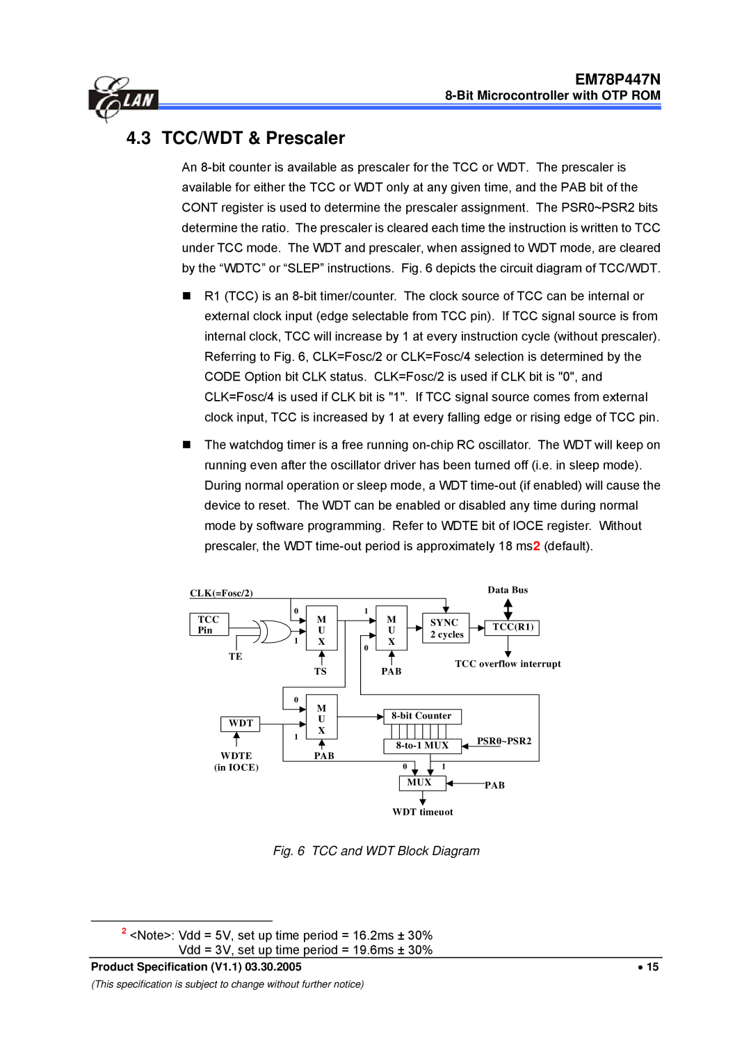
An 8-bit counter is available as prescaler for the TCC or WDT. The prescaler is available for either the TCC or WDT only at any given time, and the PAB bit of the CONT register is used to determine the prescaler assignment. The PSR0~PSR2 bits determine the ratio. The prescaler is cleared each time the instruction is written to TCC under TCC mode. The WDT and prescaler, when assigned to WDT mode, are cleared by the “WDTC” or “SLEP” instructions. Fig. 6 depicts the circuit diagram of TCC/WDT.
R1 (TCC) is an 8-bit timer/counter. The clock source of TCC can be internal or external clock input (edge selectable from TCC pin). If TCC signal source is from internal clock, TCC will increase by 1 at every instruction cycle (without prescaler). Referring to Fig. 6, CLK=Fosc/2 or CLK=Fosc/4 selection is determined by the CODE Option bit CLK status. CLK=Fosc/2 is used if CLK bit is "0", and CLK=Fosc/4 is used if CLK bit is "1". If TCC signal source comes from external clock input, TCC is increased by 1 at every falling edge or rising edge of TCC pin.
The watchdog timer is a free running on-chip RC oscillator. The WDT will keep on running even after the oscillator driver has been turned off (i.e. in sleep mode). During normal operation or sleep mode, a WDT time-out (if enabled) will cause the device to reset. The WDT can be enabled or disabled any time during normal mode by software programming. Refer to WDTE bit of IOCE register. Without prescaler, the WDT time-out period is approximately 18 ms2 (default).
0 | M | 1 | M | SYNC | |
| | TCC(R1) |
| U | | U | 2 cycles |
1 | X | | X | |
0 | | |
| | | | |
| TS | | PAB | TCC overflow interrupt |
| | | |
0 | M | | | | |
| | 8-bit Counter | |
| U | | |
1 | X | | | | PSR0~PSR2 |
| | 8-to-1 MUX |
| | |
| PAB | | |
| | 0 | 1 | |
| | | |
| | | | MUX | PAB |
WDT timeuot
Fig. 6 TCC and WDT Block Diagram
2<Note>: Vdd = 5V, set up time period = 16.2ms ± 30% Vdd = 3V, set up time period = 19.6ms ± 30%
Product Specification (V1.1) 03.30.2005 | • 15 |
(This specification is subject to change without further notice)