EM78P447N
Product Specification
8-Bit Microcontroller with OTP ROM
ELAN MICROELECTRONICS CORP
Copyright 2005 by ELAN Microelectronics Corporation
Trademark Acknowledgments
All Rights Reserved
ELAN MICROELECTRONICS CORPORATION
FEATURES
Contents
DC ELECTRICAL CHARACTERISTICS
Specification Revision History
DC Electrical Characteristic
AC Electrical Characteristic
2 FEATURES
1 GENERAL DESCRIPTION
EM78P447N
EM78P447N
Programmable free running watchdog timer
This specification is subject to change without further notice
3 PIN ASSIGNMENT
EM78P447N
Fig. 1 Pin Assignment
EM78P447N
Table 1 EM78P447NAP and EM78P447NAM Pin Description
Table 2 EM78P447NAS Pin Description
EM78P447N
Table 3 EM78P447NBP and EM78P447NBWM Pin Description
Table 4 EM78P447NCK and EN78P447NCM Pin Description
Fig. 2 Functional Block Diagram
4 FUNCTION DESCRIPTION
EM78P447N
Table 5 EM78P447NDK and EM78P447NDM Pin Description
4.1.1 R0 Indirect Addressing Register
4.1 Operational Registers
4.1.2 R1 Time Clock /Counter
4.1.3 R2 Program Counter & Stack
EM78P447N
Reset Vector
Fig. 3 Program Counter Organization
00 PAGE0 0000~03FF
EM78P447N
Fig. 4 Data Memory Configuration
4.1.6 R5~R7 Port 5 ~ Port7
4.1.5 R4 RAM Select Register
4.1.7 R8~R1F and R20~R3E General Purpose Register
EM78P447N
4.1.8 R3F Interrupt Status Register
4.2 Special Purpose Registers
4.2.1 A Accumulator
4.2.2 CONT Control Register
4.2.3 IOC5 ~ IOC7 I/O Port Control Register
4.2.4 IOCB Wake-up Control Register for Port6
EM78P447N
EM78P447N
4.2.5 IOCE WDT Control Register
4.2.6 IOCF Interrupt Mask Register
Fig. 5 Sleep Mode and Wake-Up Circuits on I/O Ports Block Diagram
EM78P447N
4.3 TCC/WDT & Prescaler
Fig. 6 TCC and WDT Block Diagram
EM78P447N
EM78P447N
4.4 I/O Ports
Fig. 7 a The I/O Port and I/O Control Register Circuit
Fig.7 b The I/O Port with R-Option P70, P71 Circuit
4.5 RESET and Wake-up
4.5.1 RESET
EM78P447N
Table 6 Usage of Sleep1 and Sleep2 Mode
EM78P447N
Table 7 The Summary of the Initialized Values for Registers
EM78P447N
0x09~0x3E
EM78P447N
EM78P447N
4.5.2 The Status of RST, T, and P of STATUS Register
4.6 Interrupt
Fig. 8 Controller Reset Block Diagram
EM78P447N
4.7.1 Oscillator Modes
4.7 Oscillator
EM78P447N
Fig. 9 Interrupt Input Circuit
EM78P447N
4.7.2 Crystal Oscillator/Ceramic ResonatorsXTAL
Fig. 10 Crystal/Resonator Circuit
Fig. 11 Crystal/Resonator Circuit
4.7.3 External RC Oscillator Mode
EM78P447N
Fig. 12 External RC Oscillator Mode Circuit
4.8 CODE Option Register
4.8.1 Code Option Register Word
EM78P447N
Bit 8 CLKS Instruction period option bit 0 two oscillator periods
EM78P447N
4.10 External Power On Reset Circuit
4.9 Power On Considerations
RESET
4.8.2 Customer ID Register Word
Vdd EM78P447N RESET
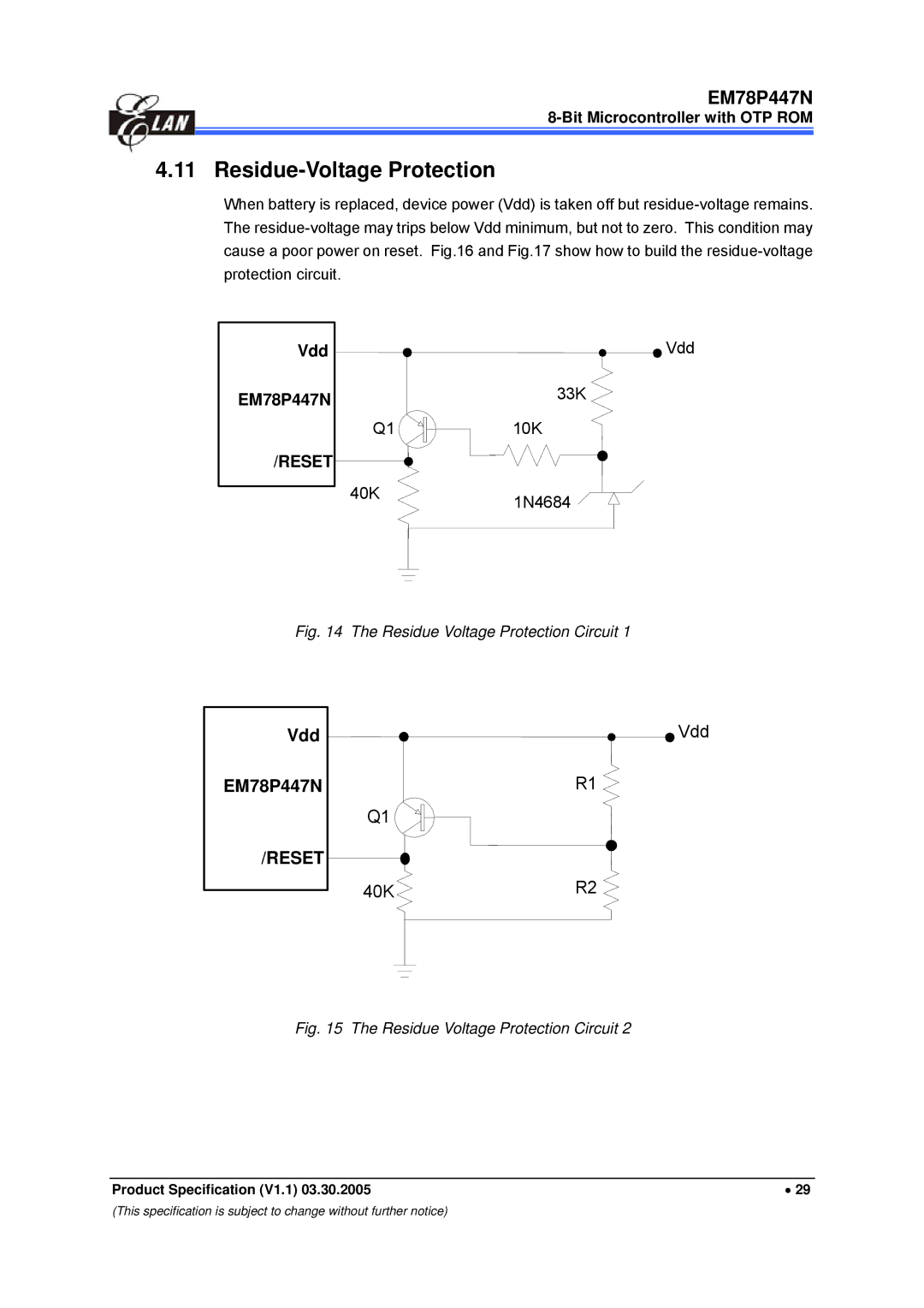
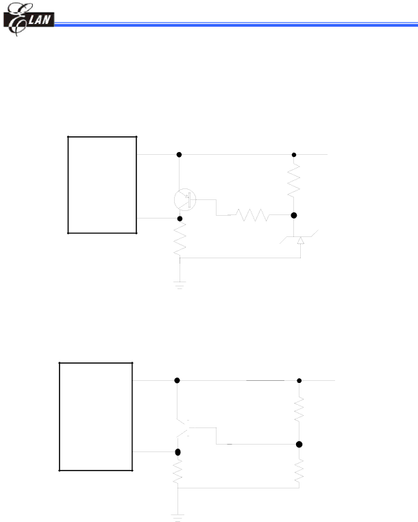
4.11 Residue-Voltage Protection
Vdd EM78P447N RESET
EM78P447N
EM78P447N
4.12 Instruction Set
INSTRUCTION
EM78P447N
MNEMONIC
OPERATION
This instruction is applicable to IOC5 ~ IOC7, IOCB, IOCE, IOCF only
EM78P447N
This instruction is not recommended for R3F operation
This instruction cannot operate under R3F
This specification is subject to change without further notice
4.13 Timing Diagram
EM78P447N
TEST POINTS
DC Electrical Characteristic
DC ELECTRICAL CHARACTERISTICS
5 ABSOLUTE MAXIMUM RATINGS
EM78P447N
EM78P447N 8-Bit Microcontroller with OTP ROM
AC Electrical Characteristic
EM78P447N
6.3 Device characteristic
EM78P447N
This specification is subject to change without further notice
Fig.18 Port5, Port6
and Port7 Voh vs. Ioh,VDD=5V
EM78P447N
This specification is subject to change without further notice
Voh/Ioh VDD=3V
IohmA
EM78P447N
This specification is subject to change without further notice
Vol/Iol VDD=5V
IolmA
EM78P447N
This specification is subject to change without further notice
Vol/Iol VDD=3V
IolmA
EM78P447N
This specification is subject to change without further notice
Vol/Iol
IolmA
EM78P447N
This specification is subject to change without further notice
Vol/Iol
IolmA
This specification is subject to change without further notice
WDT Timeout
EM78P447N
period
R=3.3k
EM78P447N
R=5.1k
R=10k
EM78P447N
ICC1:VDD=3V, Fosc=32 kHz, 2clock, WDT disable
Fig. 29 Typical Operating Current(ICC3 and ICC4) vs. Temperature
Fig. 28 Maximum Operating Current(ICC1 and ICC2) vs. Temperature
EM78P447N
Max ICC2
Temperature
Maximum ICC3 and ICC4 vs. Temperature
Fig. 30 Maximum Operating Current(ICC3 and ICC4) vs. Temperature
Fig. 31 Typical Standby Current(ISB1 and ISB2) vs. Temperature
Fig. 33 Operating Voltage In Temperature Range from -40 to
Fig. 32 Maximum Standby Current(ISB1 and ISB2) vs. Temperature
EM78P447N
Max ISB2
EM78P447N
This specification is subject to change without further notice
Fig. 34 EM78P447N I-V Curve Operating at 4 MHz
Fig. 35 EM78P447N I-V Curve Operating at 32.768 kHz
B Package Information
APPENDIX A Package Types
EM78P447N
20-Lead plastic dual inline package(DIP)- 300 mil
EM78P447N
This specification is subject to change without further notice
24-Lead plastic dual inline skinny package(DIP)- 300 mil
28-Lead plastic dual inline package(DIP)- 600 mil
EM78P447N
This specification is subject to change without further notice
32-Lead plastic dual inline package(DIP)- 600 mil
20-Lead plastic small outline package(SOP)- 300 mil
EM78P447N
This specification is subject to change without further notice
24-Lead plastic small outline package(SOP)- 300 mil
28-Lead plastic small outline package(SOP)- 300 mil
EM78P447N
This specification is subject to change without further notice
32-Lead plastic small outline package(SOP)- 300 mil
28-Lead Shrink Small Outline Package(SSOP)- 209 mil