EM78P447N
Table 5 EM78P447NDK and EM78P447NDM Pin Description
Symbol |
| Pin No. |
| Type |
| Function |
|
VDD |
| 3 |
| - |
| ■ Power supply. |
|
OSCI |
| 19 |
| I |
| ■ XTAL type: Crystal input terminal or external clock input pin. |
|
|
|
| ■ RC type: RC oscillator input pin. |
| |||
|
|
|
|
|
|
| |
|
|
|
|
|
| ■ XTAL type: Output terminal for crystal oscillator or external clock input pin. |
|
OSCO |
| 18 |
| I/O |
| ■ RC type: Instruction clock output. |
|
|
|
|
|
|
| ■ External clock signal input. |
|
TCC |
| 2 |
| I |
| ■ The real time clock/counter (with Schmitt trigger input pin) must be tied to |
|
|
|
| VDD or VSS if not in use. |
| |||
|
|
|
|
|
|
| |
/RESET |
| 20 |
| I |
| ■ Input pin with Schmitt trigger. If this pin remains at logic low, the controller |
|
|
|
| will also remain in reset condition. |
| |||
|
|
|
|
|
|
| |
P50~P54 |
| 6~9,1 |
| I/O |
| ■ P50~P54 are |
|
P60 |
| 10 |
| I/O |
| ■ P60 are |
|
|
|
| software control. |
| |||
|
|
|
|
|
|
| |
|
|
|
|
|
| ■ P74~P77 are |
|
P71~P77 |
| 11~17 |
| I/O |
| ■ P74~P75 can be |
|
|
|
| ■ P76~P77 can have |
| |||
|
|
|
|
|
|
| |
|
|
|
|
|
| ■ P71 can also be defined as the |
|
/INT |
| 5 |
| I |
| ■ External interrupt pin triggered by falling edge. |
|
VSS |
| 4 |
| - |
| ■ Ground. |
|
NC |
| 3 |
| - |
| ■ No connection. |
|
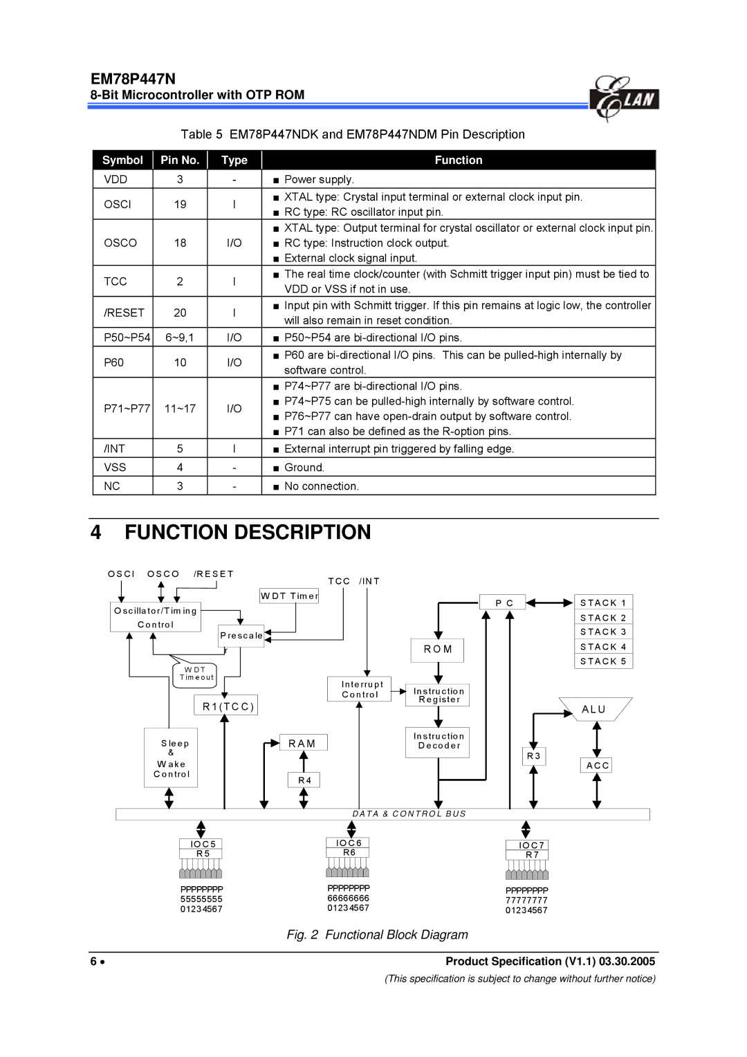
4 FUNCTION DESCRIPTION
O S C I O S C O /R E S E T |
| T C C | /IN T |
|
|
|
|
|
|
|
| ||
| W D T T im e r |
|
|
| P C | S T A C K 1 |
O s c illa to r/T im in g |
|
|
|
| ||
|
|
|
|
| S T A C K 2 | |
C o n tro l |
|
|
|
|
| |
|
|
|
|
| S T A C K 3 | |
P re s c a le |
|
|
|
| ||
|
|
|
|
| ||
r |
|
|
| R O M |
| S T A C K 4 |
W D T |
|
|
|
|
| S T A C K 5 |
|
|
|
|
|
| |
T im |
| In te rru p t |
|
|
| |
|
| In s tru c tio n |
|
| ||
|
| C o n tro l |
|
| ||
R 1 (T C C ) |
| R e g is te r |
|
| ||
|
|
|
| A L U | ||
|
|
|
|
| ||
S le e p | R A M |
|
| In s tru c tio n |
|
|
|
| D e c o d e r |
|
| ||
& |
|
|
|
| R 3 |
|
W a k e |
|
|
|
| A C C | |
|
|
|
|
| ||
C o n tro l | R 4 |
|
|
|
|
|
|
|
|
|
|
| |
|
|
| D A T A & C O N T R O L B U S |
|
| |
IO C 5 |
| IO C 6 |
| IO C 7 |
| |
R 5 |
| R6 |
| R 7 |
| |
PPPPPPPP |
| PPPPPPPP |
| PPPPPPPP |
| |
55555555 |
| 66666666 |
| 77777777 |
| |
0123 4567 |
| 0123 4567 |
| 0123 4567 |
| |
Fig. 2 Functional Block Diagram
6 • | Product Specification (V1.1) 03.30.2005 |
(This specification is subject to change without further notice)