EM78P447N
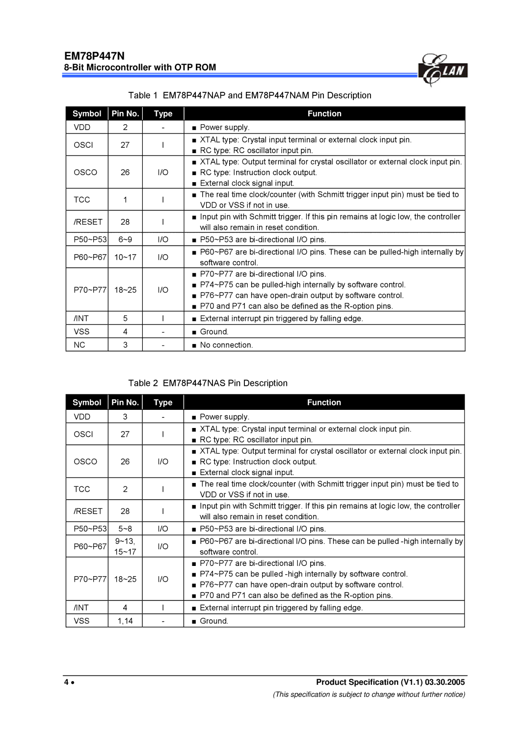
Table 1 EM78P447NAP and EM78P447NAM Pin Description
Symbol |
| Pin No. |
| Type |
| Function |
|
VDD |
| 2 |
| - |
| ■ Power supply. | |
OSCI |
| 27 |
| I |
| ■ XTAL type: Crystal input terminal or external clock input pin. | |
|
|
| ■ RC type: RC oscillator input pin. | ||||
|
|
|
|
|
| ||
|
|
|
|
|
| ■ XTAL type: Output terminal for crystal oscillator or external clock input pin. | |
OSCO |
| 26 |
| I/O |
| ■ RC type: Instruction clock output. | |
|
|
|
|
|
| ■ External clock signal input. | |
TCC |
| 1 |
| I |
| ■ The real time clock/counter (with Schmitt trigger input pin) must be tied to | |
|
|
| VDD or VSS if not in use. | ||||
|
|
|
|
|
| ||
/RESET |
| 28 |
| I |
| ■ Input pin with Schmitt trigger. If this pin remains at logic low, the controller | |
|
|
| will also remain in reset condition. | ||||
|
|
|
|
|
| ||
P50~P53 |
| 6~9 |
| I/O |
| ■ P50~P53 are | |
P60~P67 |
| 10~17 |
| I/O |
| ■ P60~P67 are | |
|
|
| software control. | ||||
|
|
|
|
|
| ||
|
|
|
|
|
| ■ P70~P77 are | |
P70~P77 |
| 18~25 |
| I/O |
| ■ P74~P75 can be | |
|
|
| ■ P76~P77 can have | ||||
|
|
|
|
|
| ||
|
|
|
|
|
| ■ P70 and P71 can also be defined as the | |
/INT |
| 5 |
| I |
| ■ External interrupt pin triggered by falling edge. | |
VSS |
| 4 |
| - |
| ■ Ground. | |
NC |
| 3 |
| - |
| ■ No connection. | |
Table 2 EM78P447NAS Pin Description
Symbol |
| Pin No. |
| Type |
| Function |
|
|
|
|
|
|
|
|
|
VDD |
| 3 |
| - |
| ■ Power supply. |
|
OSCI |
| 27 |
| I |
| ■ XTAL type: Crystal input terminal or external clock input pin. |
|
|
|
| ■ RC type: RC oscillator input pin. |
| |||
|
|
|
|
|
|
| |
|
|
|
|
|
| ■ XTAL type: Output terminal for crystal oscillator or external clock input pin. |
|
OSCO |
| 26 |
| I/O |
| ■ RC type: Instruction clock output. |
|
|
|
|
|
|
| ■ External clock signal input. |
|
TCC |
| 2 |
| I |
| ■ The real time clock/counter (with Schmitt trigger input pin) must be tied to |
|
|
|
| VDD or VSS if not in use. |
| |||
|
|
|
|
|
|
| |
/RESET |
| 28 |
| I |
| ■ Input pin with Schmitt trigger. If this pin remains at logic low, the controller |
|
|
|
| will also remain in reset condition. |
| |||
|
|
|
|
|
|
| |
P50~P53 |
| 5~8 |
| I/O |
| ■ P50~P53 are |
|
P60~P67 |
| 9~13, |
| I/O |
| ■ P60~P67 are |
|
| 15~17 |
|
| software control. |
| ||
|
|
|
|
|
| ■ P70~P77 are |
|
P70~P77 |
| 18~25 |
| I/O |
| ■ P74~P75 can be pulled |
|
|
|
| ■ P76~P77 can have |
| |||
|
|
|
|
|
|
| |
|
|
|
|
|
| ■ P70 and P71 can also be defined as the |
|
/INT |
| 4 |
| I |
| ■ External interrupt pin triggered by falling edge. |
|
VSS |
| 1,14 |
| - |
| ■ Ground. |
|
4 • | Product Specification (V1.1) 03.30.2005 |
(This specification is subject to change without further notice)