EM78P447N
Elan Microelectronics Corporation
Contents
Specification Revision History
General Description
EM78P447NBWM
PIN Assignment
EM78P447NAP and EM78P447NAM Pin Description
Symbol Pin No Type Function
EM78P447NAS Pin Description
EM78P447NBP and EM78P447NBWM Pin Description
Power supply
EM78P447NCK and EN78P447NCM Pin Description
EM78P447NDK and EM78P447NDM Pin Description
Function Description
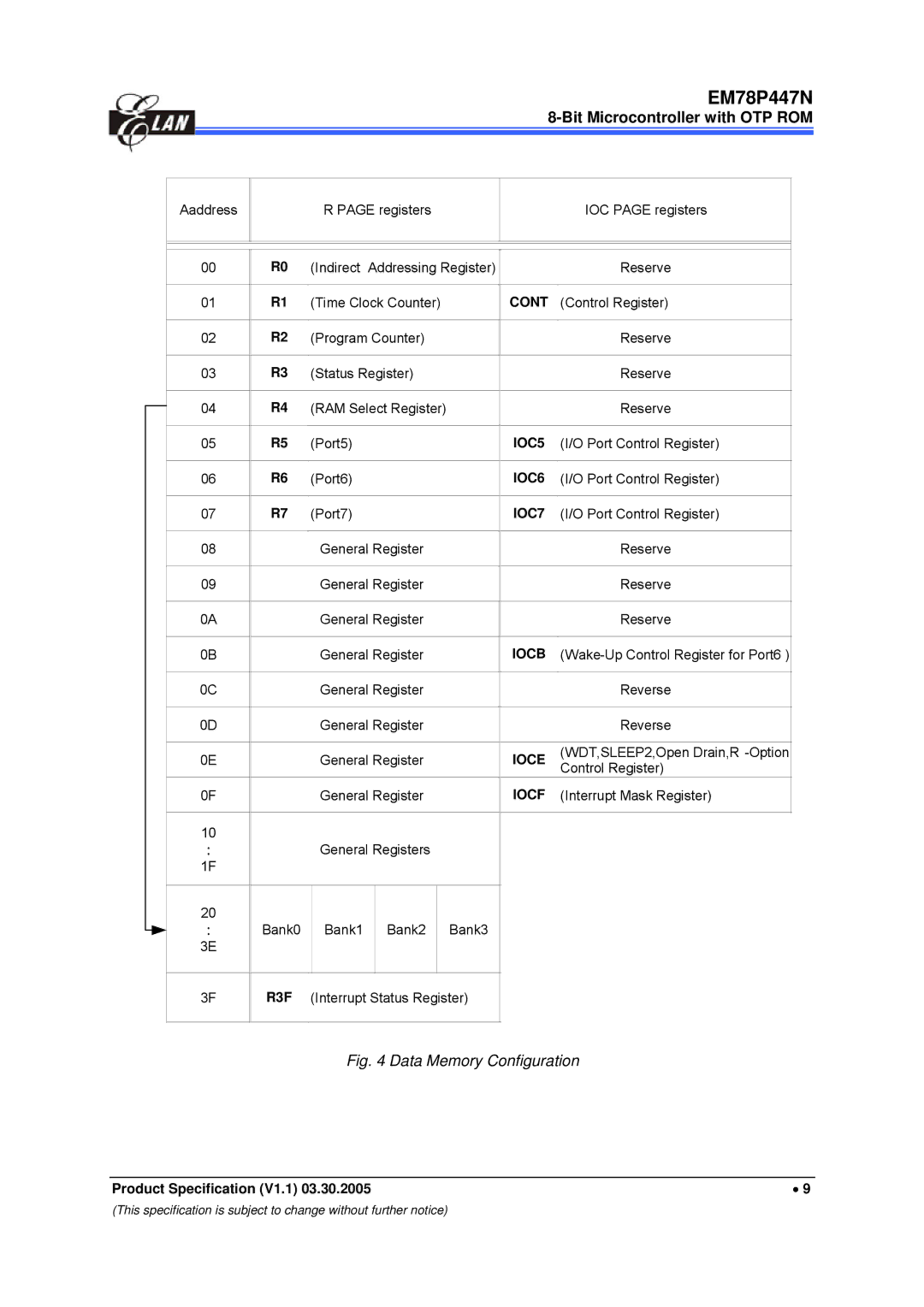
1 R0 Indirect Addressing Register
Operational Registers
2 R1 Time Clock /Counter
3 R2 Program Counter & Stack
Fffh
Call RET Retl Reti
Data Memory Configuration
6 R5~R7 Port 5 ~ Port7
5 R4 RAM Select Register
7 R8~R1F and R20~R3E General Purpose Register
R5, R6 and R7 are I/O registers
8 R3F Interrupt Status Register
Special Purpose Registers
Accumulator
Control Register
Iocb Wake-up Control Register for Port6
3 IOC5 ~ IOC7 I/O Port Control Register
TCC Rate
WDT Rate
WUE
Ioce WDT Control Register
Exie
Iocf Interrupt Mask Register
TCC/WDT & Prescaler
TCC and WDT Block Diagram
IOD
I/O Ports
Reset
Reset and Wake-up
SLEEP2 SLEEP1
Usage of Sleep1 and Sleep2 Mode
Summary of the Initialized Values for Registers
Address Name Reset Type Bit
Exif Tcif
R3FISR
WUE7 WUE6 WUE5 WUE4
Iocb
Previous value before reset
Previous status before reset
Status of RST, T, and P of Status Register
Events that may Affect the T and P Status
Interrupt
Controller Reset Block Diagram
Oscillator Modes
Oscillator
Mode
Summary of Maximum Operating Speeds
Crystal Oscillator/Ceramic ResonatorsXTAL
Conditions
Fxt max.MHz
Oscillator Type Frequency Mode C1pF C2pF
External RC Oscillator Mode
HXT
LXT
Code Option Register Word
Code Option Register
Protect
PR2~PR0 are protect bits, protect type as following
External Power On Reset Circuit
Power On Considerations
Customer ID Register Word
Bit 12~0 Customer’s ID code
Residue-Voltage Protection
Reset
Instruction Set
DAA
NOP
Contw
Slep
DJZ R
Djza R
Rrca R
RRC R
AC Test Input/Output W aveform
Timing Diagram
Symbol Parameter Condition Min Typ Max Unit
DC Electrical Characteristic
Ta= 25 C, VDD= 5.0V±5%, VSS=
Items Rating
Symbol Parameter Conditions Min Typ Max Unit
AC Electrical Characteristic
Ta=- -40 C ~ 85 C, VDD=5V ±5%, VSS=0V
Vih, Vil of TCC, /INT, /RESET Pin
Device characteristic
Port5, Port6 Port7 Voh vs. Ioh,VDD=5V
Port5, Port6, and Port7 Voh vs. Ioh, VDD=3V
Vol/Iol VDD=5V
Vol/Iol VDD=3V
Vol/Iol 100
Vol/Iol
WDT
Cext=100pF, Typical RC OSC Frequency
Typical ICC1 and ICC2 vs. Temperature
Maximum ICC1 and ICC2 vs. Temperature
Typical ISB1 and ISB2 vs. Temperature
Maximum ISB1 and ISB2 vs. Temperature
EM78P447N HXT ImA
Package Type Pin Count Package Size
Lead plastic dual inline package(DIP)- 300 mil
Lead plastic dual inline package(DIP)- 600 mil
Lead plastic dual inline skinny package(DIP)- 300 mil
838
27TYP
EM78P447N