EM78P447N
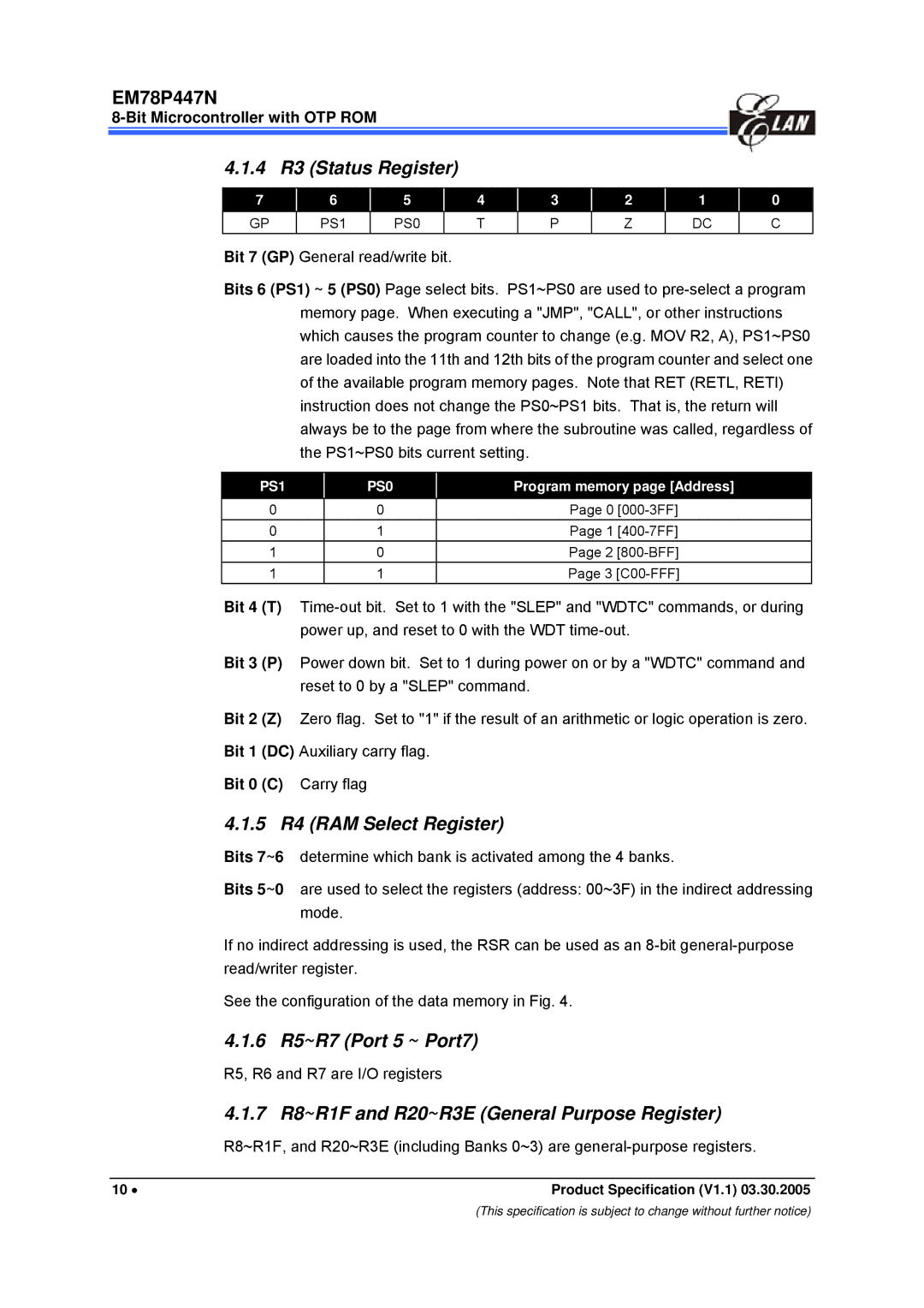
4.1.4 | R3 (Status Register) |
|
|
|
|
|
|
|
|
|
| ||||||
|
|
|
|
|
|
|
|
|
|
|
|
|
|
|
|
|
|
7 |
|
| 6 |
| 5 |
|
| 4 |
| 3 |
| 2 |
| 1 |
| 0 |
|
GP |
|
| PS1 |
| PS0 |
|
| T |
| P |
| Z |
| DC |
| C |
|
Bit 7 (GP) General read/write bit.
Bits 6 (PS1) ~ 5 (PS0) Page select bits. PS1~PS0 are used to
PS1 |
| PS0 |
| Program memory page [Address] |
|
|
|
|
|
|
|
0 |
| 0 |
| Page 0 |
|
0 |
| 1 |
| Page 1 |
|
1 |
| 0 |
| Page 2 |
|
1 |
| 1 |
| Page 3 |
|
Bit 4 (T) | ||
|
| power up, and reset to 0 with the WDT |
Bit 3 | (P) | Power down bit. Set to 1 during power on or by a "WDTC" command and |
|
| reset to 0 by a "SLEP" command. |
Bit 2 | (Z) | Zero flag. Set to "1" if the result of an arithmetic or logic operation is zero. |
Bit 1 | (DC) Auxiliary carry flag. | |
Bit 0 | (C) | Carry flag |
4.1.5 R4 (RAM Select Register)
Bits 7~6 determine which bank is activated among the 4 banks.
Bits 5~0 are used to select the registers (address: 00~3F) in the indirect addressing mode.
If no indirect addressing is used, the RSR can be used as an
See the configuration of the data memory in Fig. 4.
4.1.6 R5~R7 (Port 5 ~ Port7)
R5, R6 and R7 are I/O registers
4.1.7 R8~R1F and R20~R3E (General Purpose Register)
R8~R1F, and R20~R3E (including Banks 0~3) are
10 • | Product Specification (V1.1) 03.30.2005 |
(This specification is subject to change without further notice)