Intel 8086-1, 8086-2 manual Pin Configuration, CPU Block Diagram

Models: 8086 8086-2 8086-1

1 30
Download 30 pages 60.28 Kb
Page 1
Image 1

8086

16-BIT HMOS MICROPROCESSOR

8086/8086-2/8086-1

YDirect Addressing Capability 1 MByte of Memory

YArchitecture Designed for Powerful Assembly Language and Efficient High Level Languages

Y14 Word, by 16-Bit Register Set with Symmetrical Operations

Y24 Operand Addressing Modes

YBit, Byte, Word, and Block Operations

Y8 and 16-Bit Signed and Unsigned Arithmetic in Binary or Decimal Including Multiply and Divide

YRange of Clock Rates: 5 MHz for 8086,

8 MHz for 8086-2,

10 MHz for 8086-1

YMULTIBUS System Compatible Interface

YAvailable in EXPRESS

Standard Temperature Range

Extended Temperature Range

YAvailable in 40-Lead Cerdip and Plastic

Package

(See Packaging Spec. Order Ý231369)

The Intel 8086 high performance
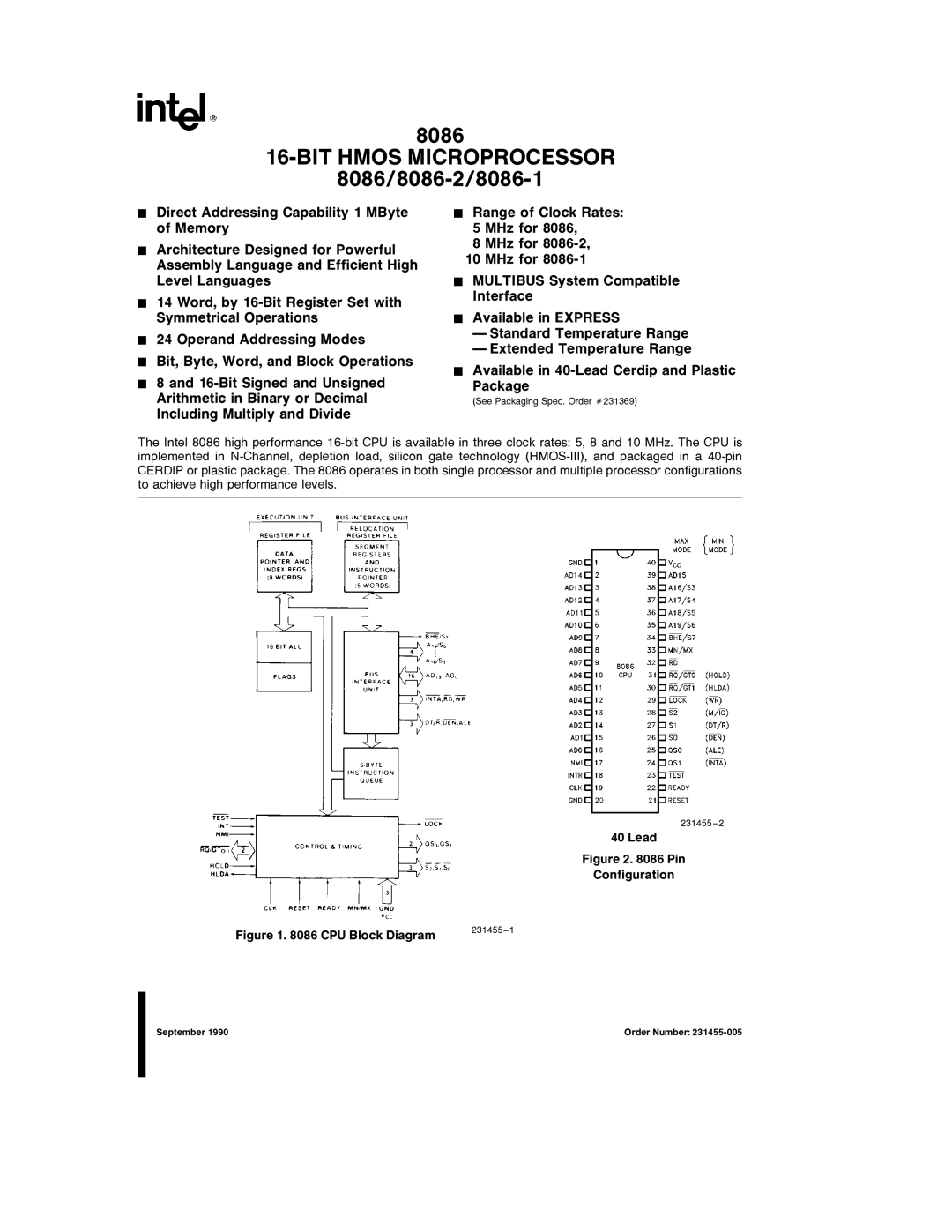
 16-bit CPU is available in three clock rates: 5, 8 and 10 MHz. The CPU is implemented in N-Channel, depletion load, silicon gate technology (HMOS-III), and packaged in a 40-pin CERDIP or plastic package. The 8086 operates in both single processor and multiple processor configurations to achieve high performance levels.

231455 – 2

40 Lead

Figure 2. 8086 Pin

Configuration

Figure 1. 8086 CPU Block Diagram

231455 – 1


September 1990

Order Number: 231455-005

Page 1
Image 1
Intel 8086-1, 8086-2 manual Pin Configuration, CPU Block Diagram