Intel 8086-1 Alternate Data extra segment, Addressing, Processor Reset and Initialization

Models: 8086 8086-2 8086-1

1 30
Download 30 pages 60.28 Kb
Page 10
Image 10

8086

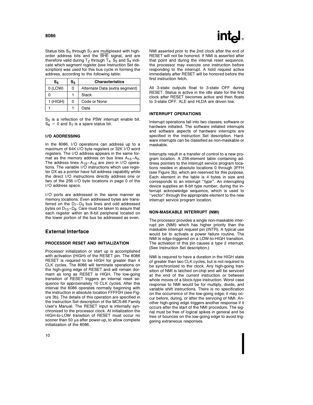
Status bits S3 through S7 are multiplexed with high- order address bits and the BHE signal, and are therefore valid during T2 through T4. S3 and S4 indi- cate which segment register (see Instruction Set de- scription) was used for this bus cycle in forming the address, according to the following table:


S4

S3

Characteristics

0

(LOW)

0

Alternate Data (extra segment)


0


1

Stack


1

(HIGH)

0

Code or None


1


1

Data


S5 is a reflection of the PSW interrupt enable bit. S6 e 0 and S7 is a spare status bit.

I/O ADDRESSING

In the 8086, I/O operations can address up to a maximum of 64K I/O byte registers or 32K I/O word registers. The I/O address appears in the same for- mat as the memory address on bus lines A15 – A0. The address lines A19 – A16 are zero in I/O opera- tions. The variable I/O instructions which use regis- ter DX as a pointer have full address capability while the direct I/O instructions directly address one or two of the 256 I/O byte locations in page 0 of the I/O address space.

I/O ports are addressed in the same manner as memory locations. Even addressed bytes are trans- ferred on the D7 – D0 bus lines and odd addressed bytes on D15 – D8. Care must be taken to assure that each register within an 8-bit peripheral located on the lower portion of the bus be addressed as even.

External Interface

PROCESSOR RESET AND INITIALIZATION

Processor initialization or start up is accomplished with activation (HIGH) of the RESET pin. The 8086 RESET is required to be HIGH for greater than 4 CLK cycles. The 8086 will terminate operations on the high-going edge of RESET and will remain dor- mant as long as RESET is HIGH. The low-going transition of RESET triggers an internal reset se- quence for approximately 10 CLK cycles. After this interval the 8086 operates normally beginning with the instruction in absolute location FFFF0H (see Fig- ure 3b). The details of this operation are specified in the Instruction Set description of the MCS-86 Family User’s Manual. The RESET input is internally syn- chronized to the processor clock. At initialization the HIGH-to-LOW transition of RESET must occur no sooner than 50 ms after power-up, to allow complete initialization of the 8086.

NMI asserted prior to the 2nd clock after the end of RESET will not be honored. If NMI is asserted after that point and during the internal reset sequence, the processor may execute one instruction before responding to the interrupt. A hold request active immediately after RESET will be honored before the first instruction fetch.

All 3-state outputs float to 3-state OFF during RESET. Status is active in the idle state for the first clock after RESET becomes active and then floats to 3-state OFF. ALE and HLDA are driven low.

INTERRUPT OPERATIONS

Interrupt operations fall into two classes; software or hardware initiated. The software initiated interrupts and software aspects of hardware interrupts are specified in the Instruction Set description. Hard- ware interrupts can be classified as non-maskable or maskable.

Interrupts result in a transfer of control to a new pro- gram location. A 256-element table containing ad- dress pointers to the interrupt service program loca- tions resides in absolute locations 0 through 3FFH (see Figure 3b), which are reserved for this purpose. Each element in the table is 4 bytes in size and corresponds to an interrupt ‘‘type’’. An interrupting device supplies an 8-bit type number, during the in- terrupt acknowledge sequence, which is used to ‘‘vector’’ through the appropriate element to the new interrupt service program location.

NON-MASKABLE INTERRUPT (NMI)

The processor provides a single non-maskable inter- rupt pin (NMI) which has higher priority than the maskable interrupt request pin (INTR). A typical use would be to activate a power failure routine. The NMI is edge-triggered on a LOW-to-HIGH transition. The activation of this pin causes a type 2 interrupt. (See Instruction Set description.)

NMI is required to have a duration in the HIGH state of greater than two CLK cycles, but is not required to be synchronized to the clock. Any high-going tran- sition of NMI is latched on-chip and will be serviced at the end of the current instruction or between whole moves of a block-type instruction. Worst case response to NMI would be for multiply, divide, and variable shift instructions. There is no specification on the occurrence of the low-going edge; it may oc- cur before, during, or after the servicing of NMI. An- other high-going edge triggers another response if it occurs after the start of the NMI procedure. The sig- nal must be free of logical spikes in general and be free of bounces on the low-going edge to avoid trig- gering extraneous responses.

10

Page 10
Image 10
Intel 8086-1, 8086-2 Alternate Data extra segment, Addressing, Processor Reset and Initialization, Interrupt Operations