CBI/CGI CB Basic
Page
Purchased
International Business Machines Corp
Table of Contents
System Bios
ISA/PCI Reference
Chassis Plans Iii
Standard Cmos Setup
Advanced Setup
This page intentionally left blank
Handling Precautions SOLDER-SIDE Components
CBI/CGI Technical Reference
Model # Model Name Speed
Chapter Specifications
CBI/CGI Technical ReferenceSpecifications
CBI BX
CGI GX
Specifications
Model # Model Name Speed CBI BX
CB Basic BX
CBI/CGI Technical Reference Specifications
Model # Model Name Speed CB Basic BX
Dram error checking and correction ECC support
SBC Block
SBC Processor Board Layout
Bios F Lash
Dimm
AGP VGA
On Basic
IDE Ultra
Humidity
Operating Temperature 0º C. to 60º C
Storage Temperature
CBI/CGI
JU9
JU7
JU8
JU18 Combo I/O P5A Reset Connect
JU15 3V Monitor Enable
JU16 Watchdog Timer
JU13
Ethernet Leds Connector Not Available
P4 Keyboard Connector
Keylock Connector
Floppy Drive Connector
Serial Port 1 Connector
Speaker Port Connector
P5A Combo I/O Connector
Serial Port 2 Connector
P9A PS/2 Mouse Header
P8 Parallel Port Connector
P9 PS/2 Mouse Connector
P11A Secondary IDE Hard Drive Connector
P10 External Reset Connector
P11 Primary IDE Hard Drive Connector
P11A Primary IDE Hard Drive Connector
P12 Hard Drive LED Connector
P13 PCI Ultra Wide Scsi Controller Connector
P19 CPU Fan
P17 Universal Serial Bus USB Connector
P18 System Hardware Monitor Connector
Pin ISA Bus Connector Component Side of Board
ISA/PCI Reference
ISA Bus connectors
ISA/PCI Reference
AEN O
IOCHK#
NOWS#
ISA/PCI Reference
Address MAP Interrupt Assignments
ISA/PCI Reference
Required Pins
PCI Pin List
Component Side of Board Volt/32-bit PCI Connector
CBI/CGI Technical Reference
Backplane
PCI Local BUS PIN Assignments
Pin Signal Name Connector Key Bit spacer
Following functional groups
CLK
PAR
STOP#
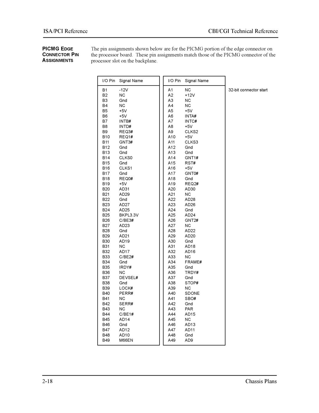
Picmg Edge
Pin Signal Name B50 Connector Key B51 B52
PAR64
System Bios
CBI/CGI Technical ReferenceSystem Bios
System Bios
Initial Power-On Screen
CBI/CGI Technical Reference System Bios
Password Entry
Bios Errors
Amibios Setup
Amibios Setup Main Menu
Amibios Hiflex Setup Utility Version
CBI/CGI Technical Reference System Bios
System Bios
CBI/CGI Technical Reference System Bios
System Bios
Mation on how to enable the Password Check option
Exit
Auto Configuration with Optimal Settings
Auto Configuration with Fail Safe Settings
Key Task Esc
This page intentionally left blank
Standard Cmos Setup
CBI/CGI Technical ReferenceStandard Cmos Setup
Standard Cmos Setup
CBI/CGI Technical Reference Standard Cmos Setup
Pri Master Auto Pri Slave Sec Master Sec Slave
User-Defined Drive Types
IDE Drive Type Setup Options
Boot Sector Virus Protection Disabled
Boot Sector Write!!! Possible Virus Continue Y/N?
Format!!! Possible Virus Continue Y/N?
Saving and Exiting
This page intentionally left blank
Menu, the following Setup screen displays
Advanced Setup
CBI/CGI Technical ReferenceAdvanced Setup
Advanced Cmos Setup Screen
Quick Boot Disabled
Advanced Setup
Quick Boot
Primary/Secondary Master/Slave Armd Emulation
CBI/CGI Technical Reference Advanced Setup
Atapi Cdrom
Floppy Access Control
Display Mode At Add-On ROM Init
Display Mode at Add-On ROM Init Force Bios
Floppy Access Control Read-Write
A.R.T. for Hard Disks Disabled
Hard Disk Access Control
Hard Disk Access Control Read-Write
BootUp Num-Lock
VGA/EGA
Parity Check
Parity Check Enabled
Boot To OS/2
Internal Cache
External Cache
System Bios Cacheable
System Bios Cacheable Enabled
External Cache WriteBack
XXXX,16K Shadow Cached
This page intentionally left blank
CBI/CGI Technical Reference Advanced Setup
Advanced Chipset Setup Screen
USB Function
USB Function Enabled
Port 64/60 Emulation Disabled
USB Keyboard/Mouse Legacy Support
SERR#
PERR#
PCI1 to PCI0 Access
Multi-Transaction Timer Clks
Multi-Trans Timer Clks
PCI1 to PCI0 Access Enabled
Memory Hole
Memory Hole Disabled
Dram Refresh Rate
Graphics Aperture Size not available on Basic models
AGP Mlti-Trans Timer AGP Clks
AGP Low-Priority Timer AGP Clks
Graphics Aperture Size 64MB
AGP Serr
PIIX4 SERR#
DMA-0 through DMA-7 Type
PIIX4 Delayed Transaction Enabled
Type F DMA Buffer Control1/Type Fdma Buffer Control2
DMA-# Type Normal ISA
This page intentionally left blank
Power Management Setup Screen
Chapter Power Management Setup
CBI/CGI Technical ReferencePower Management Setup
Acpi Aware O/S
Power Management Setup
Hard Disk Power Down Mode
Video Power Down Mode
Video Power Down Mode Disabled
Hard Disk Power Down Mode Disabled
POS
Slow Clock Ratio 50%-62.5%
Suspend Time Out Disabled
Suspend Time Out
Display Activity
Device 0 through Device 8 Monitoring
PCI/Plug and Play Setup Screen
Chapter PCI/Plug and Play Setup
CBI/CGI Technical ReferencePCI/Plug and Play Setup
PCI/Plug and Play Setup
On Board LAN not available on Basic models
PCI VGA Palette Snoop Disabled
CBI/CGI Technical Reference PCI/Plug and Play Setup
PCI Latency Timer PCI Clocks
PCI VGA Palette Snoop
OffBoard PCI IDE Card Auto
PCI IDE BusMaster Disabled
OffBoard PCI IDE Card
OffBoard PCI IDE Primary IRQ/Secondary IRQ
IRQ5/IRQ9/IRQ10/IRQ11/IRQ15
DMA Channels 0, 1, 3, 5, 6
DMA Channel # PnP
IRQ#PCI/PnP
Reserved Memory Address
Reserved Memory Size Disabled
Reserved Memory Size
Peripheral Setup Screen
Chapter Peripheral Setup
CBI/CGI Technical ReferencePeripheral Setup
OnBoard FDC Auto
Peripheral Setup
OnBoard FDC
OnBoard Serial Port 1/OnBoard Serial Port
OnBoard Parallel Port
CBI/CGI Technical Reference Peripheral Setup
Parallel Port Mode
OnBoard Parallel Port Auto
Parallel Port IRQ Auto
EPP Version
Parallel Port IRQ
Parallel Port DMA Channel
OnBoard IDE
OnBoard IDEBoth
This page intentionally left blank
Appendix a Bios Messages
Bios Error
Correct the error, run the Bios Setup Utility
OFF Board Parity Error
ISA Bios NMI
Uncompressed Initialization Code Checkpoints
Port 80 Codes
CBI/CGI Technical Reference
Point 4EH next
Extended NMI sources enabling in progress
Displaying any soft errors next
Is being executed in different buses
Appendix B Adaptec, Inc. Software License
CBI/CGI Technical Reference
Appendix C SCSISelect Configuration Utility
Scsiselect
Save Changes Made? Yes
Options Screen
Configure/View Host Adapter Settings Screen
Host Adapter Scsi ID
Scsi Parity Checking
Host Adapter Scsi Termination
Bit Adapter Termination Settings
Boot LUN Number
Boot Device Configuration Screen
Boot Target ID
Scsi Device
Described below Initiate Sync Negotiation
Enable Disconnection
Maximum Sync Transfer Rate
Send Start Unit Command
Initiate Wide Negotiation
Include in Bios Scan
Plug and Play Scam Support
Adapter Settings Menu, the following screen displays
Advanced Configuration Options Screen
Support Removable Disks Under Bios as Fixed Disks
Reset Scsi Bus at IC Initialization
Host Adapter Bios
Multiple LUN Support
Extended Bios Translation for DOS Drives 1 GByte
Display Ctrl-A Message During Bios Initialization
Support for Ultra Scsi Speed
Bios Support for Bootable CD-ROM
Bios Support for Int 13H Extensions
Scsi Disk Utilities Screen
Format Disk
Verify Disk Media
CBI/CGI Technical Reference
89/336/EEC
Declaration of Conformity
Application of Council Directives
EN55022 1994/A21997, Class a EN50082-2
This page intentionally left blank