MAX12527
Dual, 65Msps, 12-Bit, IF/Baseband ADC
|
|
| Pin Description | ||
|
|
|
|
| |
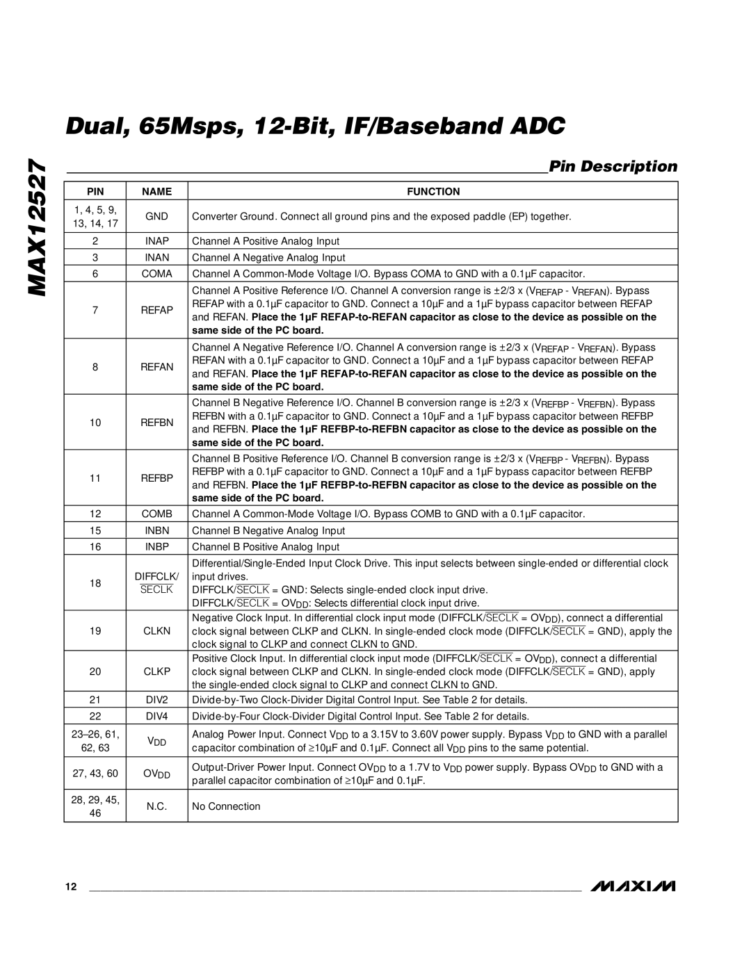
| PIN | NAME | FUNCTION | ||
1, 4, 5, 9, | GND | Converter Ground. Connect all ground pins and the exposed paddle (EP) together. | |||
13, 14, 17 | |||||
|
|
| |||
|
|
|
|
| |
2 | INAP | Channel A Positive Analog Input | |||
|
|
|
|
| |
3 | INAN | Channel A Negative Analog Input | |||
|
|
|
|
| |
6 | COMA | Channel A | |||
|
|
| Channel A Positive Reference I/O. Channel A conversion range is ±2/3 x (VREFAP - VREFAN). Bypass | ||
7 | REFAP | REFAP with a 0.1µF capacitor to GND. Connect a 10µF and a 1µF bypass capacitor between REFAP | |||
and REFAN. Place the 1µF | |||||
|
|
| |||
|
|
| same side of the PC board. | ||
|
|
|
|
| |
|
|
| Channel A Negative Reference I/O. Channel A conversion range is ±2/3 x (VREFAP - VREFAN). Bypass | ||
8 | REFAN | REFAN with a 0.1µF capacitor to GND. Connect a 10µF and a 1µF bypass capacitor between REFAP | |||
and REFAN. Place the 1µF | |||||
|
|
| |||
|
|
| same side of the PC board. | ||
|
|
| Channel B Negative Reference I/O. Channel B conversion range is ±2/3 x (VREFBP - VREFBN). Bypass | ||
10 | REFBN | REFBN with a 0.1µF capacitor to GND. Connect a 10µF and a 1µF bypass capacitor between REFBP | |||
and REFBN. Place the 1µF | |||||
|
|
| |||
|
|
| same side of the PC board. | ||
|
|
| Channel B Positive Reference I/O. Channel B conversion range is ±2/3 x (VREFBP - VREFBN). Bypass | ||
11 | REFBP | REFBP with a 0.1µF capacitor to GND. Connect a 10µF and a 1µF bypass capacitor between REFBP | |||
and REFBN. Place the 1µF | |||||
|
|
| |||
|
|
| same side of the PC board. | ||
12 | COMB | Channel A | |||
|
|
|
|
| |
15 | INBN | Channel B Negative Analog Input | |||
|
|
|
|
| |
16 | INBP | Channel B Positive Analog Input | |||
|
|
|
|
| |
|
|
| |||
18 | DIFFCLK/ | input drives. | |||
SECLK | DIFFCLK/SECLK = GND: Selects | ||||
|
| ||||
|
|
| DIFFCLK/SECLK = OVDD: Selects differential clock input drive. | ||
19 | CLKN | Negative Clock Input. In differential clock input mode (DIFFCLK/SECLK = OVDD), connect a differential | |||
clock signal between CLKP and CLKN. In | |||||
|
|
| clock signal to CLKP and connect CLKN to GND. | ||
20 | CLKP | Positive Clock Input. In differential clock input mode (DIFFCLK/SECLK = OVDD), connect a differential | |||
clock signal between CLKP and CLKN. In | |||||
|
|
| the | ||
21 | DIV2 | ||||
|
|
|
|
| |
22 | DIV4 | ||||
|
|
|
|
| |
| VDD | Analog Power Input. Connect VDD to a 3.15V to 3.60V power supply. Bypass VDD to GND with a parallel | |||
62, 63 | capacitor combination of ≥10µF and 0.1µF. Connect all VDD pins to the same potential. | ||||
| |||||
27, 43, 60 | OVDD | ||||
parallel capacitor combination of ≥10µF and 0.1µF. | |||||
|
|
| |||
|
|
|
|
| |
28, 29, 45, | N.C. | No Connection | |||
46 | |||||
|
|
| |||
|
|
|
|
| |
12 ______________________________________________________________________________________