Bypass REFIN and REFOUT to GND with a 0.1µF capac-
itor. The REFIN input impedance is very large (>50M).
When driving REFIN through a resistive divider, use
resistances 10kto avoid loading REFOUT.
Buffered external reference mode is virtually identical to
the internal reference mode except that the reference
source is derived from an external reference and not the
MAX12527’s internal bandgap reference. In buffered
external reference mode, apply a stable reference volt-
age source between 0.7V to 2.3V at REFIN. Pins COM_,
REF_P, and REF_N are low-impedance outputs with
VCOM_ = VDD / 2, VREF_P = VDD / 2 + 3/8 x VREFIN, and
VREF_N = VDD / 2 - 3/8 x VREFIN. Bypass REF_P, REF_N,
and COM_ each with a 0.1µF capacitor to GND. Bypass
REF_P to REF_N with a 10µF capacitor.
Connect REFIN to GND to enter unbuffered external ref-
erence mode. Connecting REFIN to GND deactivates
the on-chip reference buffers for COM_, REF_P, and
REF_N. With their buffers deactivated, COM_, REF_P,
and REF_N become high-impedance inputs and must
be driven with separate, external reference sources.
Drive VCOM_ to VDD / 2 ±5%, and drive REF_P and
REF_N so VCOM_ = (VREF_P_ + VREF_N_) / 2. The analog
input range is ±(VREF_P_ - VREF_N) x 2/3. Bypass
REF_P, REF_N, and COM_ each with a 0.1µF capacitor
to GND. Bypass REF_P to REF_N with a 10µF capacitor.
For all reference modes, bypass REFOUT with a 0.1µF
and REFIN with a 4.7µF capacitor to GND.
The MAX12527 also features a shared reference mode,
in which the user can achieve better channel-to-chan-
nel matching. When sharing the reference (SHREF =
VDD), externally connect REFAP and REFBP together to
ensure that VREFAP = VREFBP. Similarly, when sharing
the reference, externally connect REFAN to REFBN
together to ensure that VREFAN = VREFBN.
Connect SHREF to GND to disable the shared refer-
ence mode of the MAX12527. In this independent refer-
ence mode, a better channel-to-channel isolation is
achieved.
For detailed circuit suggestions and how to drive the
ADC in buffered/unbuffered external reference mode,
see the Applications Information section.
Clock Duty-Cycle Equalizer
The MAX12527 has an internal clock duty-cycle equaliz-
er, which makes the converter insensitive to the duty
cycle of the signal applied to CLKP and CLKN. The con-
verters allow clock duty-cycle variations from 25% to 75%
without negatively impacting the dynamic performance.
The clock duty-cycle equalizer uses a delay-locked
loop (DLL) to create internal timing signals that are
duty-cycle independent. Due to this DLL, the
MAX12527 requires approximately 100 clock cycles to
acquire and lock to new clock frequencies.
Clock Input and Clock Control Lines
The MAX12527 accepts both differential and single-
ended clock inputs with a wide 25% to 75% input clock
duty cycle. For single-ended clock input operation,
connect DIFFCLK/SECLK and CLKN to GND. Apply an
external single-ended clock signal to CLKP. To reduce
clock jitter, the external single-ended clock must have
sharp falling edges. For differential clock input opera-
tion, connect DIFFCLK/SECLK to OVDD. Apply an
external differential clock signal to CLKP and CLKN.
Consider the clock input as an analog input and route it
away from any other analog inputs and digital signal
lines. CLKP and CLKN enter high impedance when the
MAX12527 is powered down (Figure 4).
Low clock jitter is required for the specified SNR perfor-
mance of the MAX12527. The analog inputs are sam-
pled on the falling (rising) edge of CLKP (CLKN),
requiring this edge to have the lowest possible jitter.
Jitter limits the maximum SNR performance of any ADC
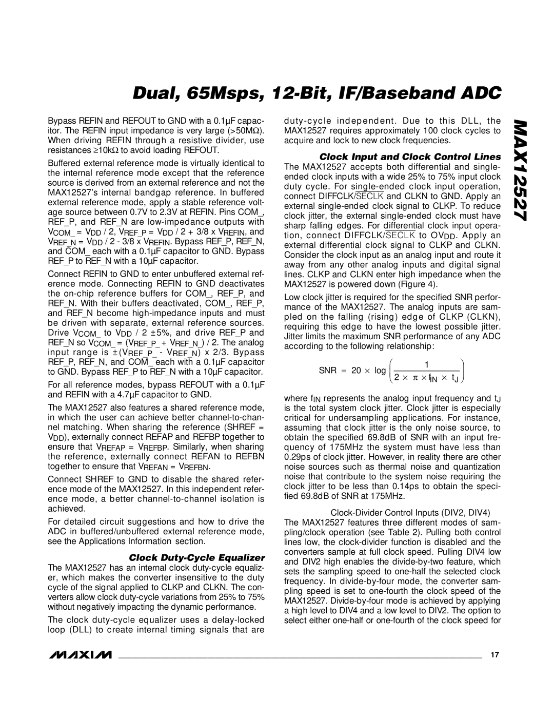
according to the following relationship:
where fIN represents the analog input frequency and tJ
is the total system clock jitter. Clock jitter is especially
critical for undersampling applications. For instance,
assuming that clock jitter is the only noise source, to
obtain the specified 69.8dB of SNR with an input fre-
quency of 175MHz the system must have less than
0.29ps of clock jitter. However, in reality there are other
noise sources such as thermal noise and quantization
noise that contribute to the system noise requiring the
clock jitter to be less than 0.14ps to obtain the speci-
fied 69.8dB of SNR at 175MHz.
Clock-Divider Control Inputs (DIV2, DIV4)
The MAX12527 features three different modes of sam-
pling/clock operation (see Table 2). Pulling both control
lines low, the clock-divider function is disabled and the
converters sample at full clock speed. Pulling DIV4 low
and DIV2 high enables the divide-by-two feature, which
sets the sampling speed to one-half the selected clock
frequency. In divide-by-four mode, the converter sam-
pling speed is set to one-fourth the clock speed of the
MAX12527. Divide-by-four mode is achieved by applying
a high level to DIV4 and a low level to DIV2. The option to
select either one-half or one-fourth of the clock speed for
SNR ft
IN J
log
×××
20 1
2π
MAX12527
Dual, 65Msps, 12-Bit, IF/Baseband ADC
______________________________________________________________________________________ 17