Dual, 65Msps, 12-Bit, IF/Baseband ADC
MAX12527 | BOND WIRE | VDD |
| |
|
| |||
INDUCTANCE |
| MAX12527 | ||
1.5nH |
| |||
|
| |||
IN_P | CPAR | *CSAMPLE | ||
| ||||
| 2pF | 4.5pF | ||
BOND WIRE | VDD |
| ||
|
| |||
INDUCTANCE |
|
| ||
1.5nH |
|
| ||
IN_N | CPAR | *CSAMPLE | ||
| ||||
|
| |||
|
| 2pF | 4.5pF | |
| SAMPLING |
|
| |
| CLOCK |
|
| |
| *THE EFFECTIVE RESISTANCE OF THE | 1 | ||
| SWITCHED SAMPLING CAPACITORS IS: RIN = | |||
| fCLK x CSAMPLE | |||
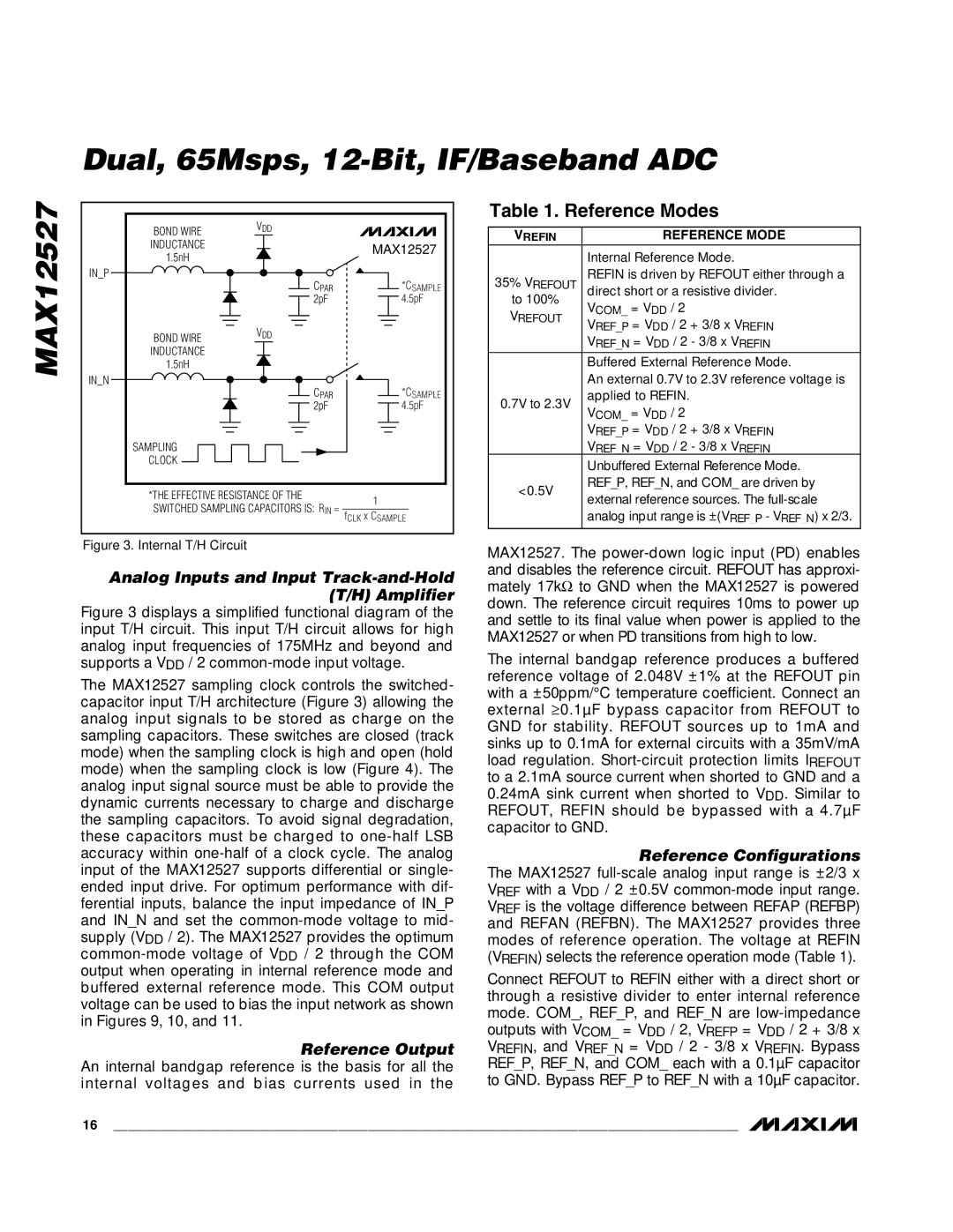
Figure 3. Internal T/H Circuit
Analog Inputs and Input Track-and-Hold (T/H) Amplifier
Figure 3 displays a simplified functional diagram of the input T/H circuit. This input T/H circuit allows for high analog input frequencies of 175MHz and beyond and supports a VDD / 2 common-mode input voltage.
The MAX12527 sampling clock controls the switched- capacitor input T/H architecture (Figure 3) allowing the analog input signals to be stored as charge on the sampling capacitors. These switches are closed (track mode) when the sampling clock is high and open (hold mode) when the sampling clock is low (Figure 4). The analog input signal source must be able to provide the dynamic currents necessary to charge and discharge the sampling capacitors. To avoid signal degradation, these capacitors must be charged to one-half LSB accuracy within one-half of a clock cycle. The analog input of the MAX12527 supports differential or single- ended input drive. For optimum performance with dif- ferential inputs, balance the input impedance of IN_P and IN_N and set the common-mode voltage to mid- supply (VDD / 2). The MAX12527 provides the optimum common-mode voltage of VDD / 2 through the COM output when operating in internal reference mode and buffered external reference mode. This COM output voltage can be used to bias the input network as shown in Figures 9, 10, and 11.
Reference Output
An internal bandgap reference is the basis for all the internal voltages and bias currents used in the
Table 1. Reference Modes
VREFIN | REFERENCE MODE | |
| Internal Reference Mode. | |
35% VREFOUT | REFIN is driven by REFOUT either through a | |
direct short or a resistive divider. | ||
to 100% | VCOM_ = VDD / 2 | |
VREFOUT | ||
VREF_P = VDD / 2 + 3/8 x VREFIN | ||
| ||
| VREF_N = VDD / 2 - 3/8 x VREFIN | |
|
| |
| Buffered External Reference Mode. | |
| An external 0.7V to 2.3V reference voltage is | |
0.7V to 2.3V | applied to REFIN. | |
VCOM_ = VDD / 2 | ||
| ||
| VREF_P = VDD / 2 + 3/8 x VREFIN | |
| VREF_N = VDD / 2 - 3/8 x VREFIN | |
| Unbuffered External Reference Mode. | |
<0.5V | REF_P, REF_N, and COM_ are driven by | |
external reference sources. The | ||
| ||
| analog input range is ±(VREF_P - VREF_N) x 2/3. |
MAX12527. The
The internal bandgap reference produces a buffered reference voltage of 2.048V ±1% at the REFOUT pin with a ±50ppm/°C temperature coefficient. Connect an external ≥0.1µF bypass capacitor from REFOUT to GND for stability. REFOUT sources up to 1mA and sinks up to 0.1mA for external circuits with a 35mV/mA load regulation.
Reference Configurations
The MAX12527
Connect REFOUT to REFIN either with a direct short or through a resistive divider to enter internal reference mode. COM_, REF_P, and REF_N are
16 ______________________________________________________________________________________