Dual, 65Msps, 12-Bit, IF/Baseband ADC
externally isolates it from heavy capacitive loads. Refer to the MAX12527 EV Kit schematic for recommendations of how to drive the DAV signal through an external buffer.
Data
V ) x 2/3. Signals outside of this valid differential range cause DOR_ to assert high as shown in Table 1.
DOR is synchronized with DAV and transitions along with the output data
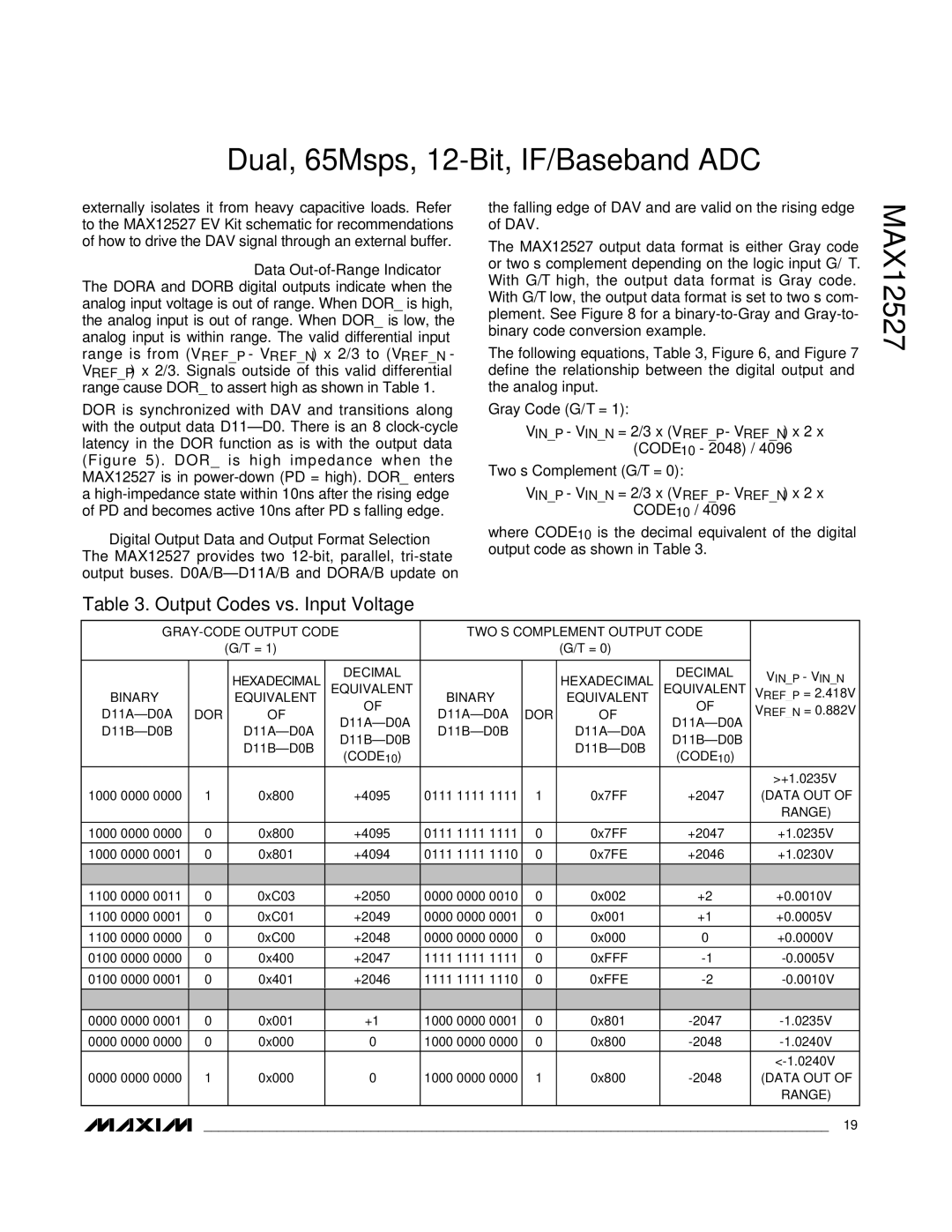
Digital Output Data and Output Format Selection The MAX12527 provides two
the falling edge of DAV and are valid on the rising edge of DAV.
The MAX12527 output data format is either Gray code or two’s complement depending on the logic input G/T. With G/T high, the output data format is Gray code. With G/T low, the output data format is set to two’s com- plement. See Figure 8 for a
The following equations, Table 3, Figure 6, and Figure 7 define the relationship between the digital output and the analog input.
Gray Code (G/T = 1):
VIN_P - VIN_N = 2/3 x (VREF_P - VREF_N) x 2 x
(CODE10 - 2048) / 4096
Two’s Complement (G/T = 0):
VIN_P - VIN_N = 2/3 x (VREF_P - VREF_N) x 2 x CODE10 / 4096
where CODE10 is the decimal equivalent of the digital output code as shown in Table 3.
MAX12527
Table 3. Output Codes vs. Input Voltage
TWO’S COMPLEMENT OUTPUT CODE |
| ||||||||
|
| (G/T = 1) |
|
|
| (G/T = 0) |
|
| |
|
|
|
|
|
|
|
|
| |
|
| HEXADECIMAL | DECIMAL |
|
| HEXADECIMAL | DECIMAL | VIN_P - VIN_N | |
|
| EQUIVALENT |
|
| EQUIVALENT | ||||
BINARY |
| EQUIVALENT | BINARY |
| EQUIVALENT | VREF_P = 2.418V | |||
| DOR | OF | OF | DOR | OF | OF | VREF_N = 0.882V | ||
| |||||||||
|
|
|
| ||||||
|
|
| |||||||
|
|
|
|
| |||||
|
| (CODE10) |
|
| (CODE10) |
| |||
|
|
|
|
|
|
| |||
|
|
|
|
|
|
|
| >+1.0235V | |
1000 0000 0000 | 1 | 0x800 | +4095 | 0111 1111 1111 | 1 | 0x7FF | +2047 | (DATA OUT OF | |
|
|
|
|
|
|
|
| RANGE) | |
|
|
|
|
|
|
|
|
| |
1000 0000 0000 | 0 | 0x800 | +4095 | 0111 1111 1111 | 0 | 0x7FF | +2047 | +1.0235V | |
|
|
|
|
|
|
|
|
| |
1000 0000 0001 | 0 | 0x801 | +4094 | 0111 1111 1110 | 0 | 0x7FE | +2046 | +1.0230V | |
|
|
|
|
|
|
|
|
| |
|
|
|
|
|
|
|
|
| |
1100 0000 0011 | 0 | 0xC03 | +2050 | 0000 0000 0010 | 0 | 0x002 | +2 | +0.0010V | |
|
|
|
|
|
|
|
|
| |
1100 0000 0001 | 0 | 0xC01 | +2049 | 0000 0000 0001 | 0 | 0x001 | +1 | +0.0005V | |
|
|
|
|
|
|
|
|
| |
1100 0000 0000 | 0 | 0xC00 | +2048 | 0000 0000 0000 | 0 | 0x000 | 0 | +0.0000V | |
0100 0000 0000 | 0 | 0x400 | +2047 | 1111 1111 1111 | 0 | 0xFFF | |||
|
|
|
|
|
|
|
|
| |
0100 0000 0001 | 0 | 0x401 | +2046 | 1111 1111 1110 | 0 | 0xFFE | |||
|
|
|
|
|
|
|
|
| |
|
|
|
|
|
|
|
|
| |
0000 0000 0001 | 0 | 0x001 | +1 | 1000 0000 0001 | 0 | 0x801 | |||
|
|
|
|
|
|
|
|
| |
0000 0000 0000 | 0 | 0x000 | 0 | 1000 0000 0000 | 0 | 0x800 | |||
|
|
|
|
|
|
|
|
| |
|
|
|
|
|
|
|
| ||
0000 0000 0000 | 1 | 0x000 | 0 | 1000 0000 0000 | 1 | 0x800 | (DATA OUT OF | ||
|
|
|
|
|
|
|
| RANGE) | |
|
|
|
|
|
|
|
|
| |
______________________________________________________________________________________ 19