Dual, 65Msps, 12-Bit, IF/Baseband ADC
MAX12527
VDD |
| |
S1H | MAX12527 | |
| ||
10kΩ |
| |
CLKP |
| |
10kΩ | ||
S2H | ||
| EQUALIZER | |
S1L | 10kΩ | |
| ||
CLKN |
| |
| 10kΩ | |
| SWITCHES S1_ AND S2_ ARE OPEN | |
S2L | DURING | |
| CLKP AND CLKN HIGH IMPEDANCE. | |
GND | SWITCHES S2_ ARE OPEN IN | |
|
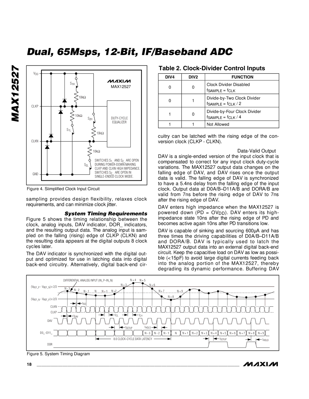
Figure 4. Siimplified Clock Input Circuit
sampling provides design flexibility, relaxes clock requirements, and can minimize clock jitter.
System Timing Requirements
Figure 5 shows the timing relationship between the clock, analog inputs, DAV indicator, DOR_ indicators, and the resulting output data. The analog input is sam- pled on the falling (rising) edge of CLKP (CLKN) and the resulting data appears at the digital outputs 8 clock cycles later.
The DAV indicator is synchronized with the digital out- put and optimized for use in latching data into digital back-end circuitry. Alternatively, digital back-end cir-
Table 2. Clock-Divider Control Inputs
DIV4 | DIV2 | FUNCTION | |
|
|
| |
0 | 0 | Clock Divider Disabled | |
fSAMPLE = fCLK | |||
|
| ||
|
|
| |
0 | 1 | ||
fSAMPLE = fCLK / 2 | |||
|
| ||
|
|
| |
1 | 0 | ||
fSAMPLE = fCLK / 4 | |||
|
| ||
|
|
| |
1 | 1 | Not Allowed | |
|
|
|
cuitry can be latched with the rising edge of the con- version clock (CLKP - CLKN).
Data-Valid Output
DAV is a
DAV enters high impedance when the MAX12527 is powered down (PD = OVDD). DAV enters its high- impedance state 10ns after the rising edge of PD and becomes active again 10ns after PD transitions low.
DAV is capable of sinking and sourcing 600µA and has three times the driving capabilities of
| DIFFERENTIAL ANALOG INPUT | N + 4 | N + 5 |
|
|
|
|
|
|
|
|
|
|
| ||||
(VREF_P - VREF_N) x 2/3 | N - 3 |
|
|
|
| N + 3 | N + 6 |
|
|
|
|
|
|
|
|
|
|
|
N - 2 |
|
|
|
|
|
|
|
|
|
|
|
|
|
|
|
| ||
| N - 1 | N | N + 1 N +2 | N + 7 |
| N + 9 |
|
|
|
|
|
|
|
| ||||
|
|
|
|
|
|
|
|
|
|
| ||||||||
|
|
|
|
|
|
|
|
|
|
|
| |||||||
(VREF_N - VREF_P) x 2/3 |
|
|
|
|
|
|
| N + 8 |
|
|
|
|
|
|
|
|
|
|
|
|
|
|
|
|
|
|
|
|
|
|
|
|
|
|
|
| |
CLKN |
|
| tAD |
|
|
|
|
|
|
|
|
|
|
|
|
|
|
|
|
|
|
|
|
|
|
|
|
|
|
|
|
|
|
|
|
| |
CLKP |
| tDAV |
|
|
| tCL | tCH |
|
|
|
|
|
|
|
|
|
|
|
|
|
|
|
|
|
|
|
|
|
|
|
|
|
|
| |||
DAV |
|
|
|
|
|
|
|
|
|
|
|
|
|
|
|
|
|
|
|
|
|
|
|
| tSETUP | tHOLD |
|
|
|
|
|
|
|
|
|
|
|
|
|
|
|
|
| N - 3 N - 2 | N - 1 | N | N + 1 | N + 2 | N + 3 | N + 4 | N + 5 | N + 6 | N + 7 | N + 8 | N + 9 | |
|
|
|
|
|
| 8.0 |
|
|
|
|
|
| tSETUP |
|
|
| tHOLD | |
DOR |
|
|
|
|
|
|
|
|
|
|
|
|
|
|
|
|
|
|
Figure 5. System Timing Diagram
18 ______________________________________________________________________________________