| Dual, 65Msps, |
|
| |||||||
MAX12527 | 3.3V |
|
|
|
|
|
|
|
|
|
0.1µF |
| 3V |
|
|
|
|
| 0.1µF | 2.2µF | |
1 |
|
|
|
|
|
| ||||
5 |
|
|
|
|
|
|
| |||
|
|
|
|
|
|
|
|
| ||
|
| 20kΩ |
|
|
|
| REF_P | VDD |
| |
| MAX6029 | 1% |
|
|
|
|
|
| ||
|
|
|
|
| 0.1µF |
| REFOUT |
| ||
| (EUK30) |
|
|
|
|
|
| |||
|
|
|
|
|
|
|
| 0.1µF | ||
|
| 20kΩ |
|
|
| 10µF | 0.1µF |
| ||
|
|
|
|
|
|
| ||||
| 2 | 1% |
|
| 2.413V |
| MAX12527 |
| ||
|
| 1 |
|
|
| |||||
|
|
|
|
|
|
|
| |||
|
|
| 4 | 47Ω |
|
| REF_N |
|
| |
|
|
|
|
|
|
|
| |||
|
|
|
|
|
| 0.1µF |
|
|
| |
|
|
|
| MAX4230 |
|
|
|
|
| |
|
|
|
|
|
|
|
|
|
| |
|
| 0.47µF |
| 3 |
| 330µF |
|
|
|
|
|
|
| 10µF |
|
|
|
|
| ||
|
|
|
| 6V | 1.47kΩ | 6V |
|
|
|
|
|
|
| 52.3kΩ |
|
|
| COM_ | REFIN |
| |
|
|
|
|
|
|
|
| |||
|
|
| 1% |
|
|
| 0.1µF |
| GND |
|
|
|
|
|
|
| 1.647V |
|
|
| |
|
|
|
| 1 |
|
|
|
|
| |
|
|
|
| 4 | 47Ω |
|
|
|
|
|
|
|
|
|
|
|
|
|
|
| |
|
|
|
| MAX4230 |
|
|
| 3.3V |
|
|
|
|
|
| 3 |
| 330µF |
|
|
|
|
|
|
|
| 10µF |
|
|
|
|
| |
|
|
| 52.3kΩ | 6V | 1.47kΩ | 6V |
|
|
|
|
|
|
|
|
|
|
|
|
| ||
|
|
| 1% |
|
|
|
| 0.1µF | 2.2µF | |
|
|
|
|
|
|
|
| |||
|
|
|
|
|
|
|
|
| ||
|
|
|
| 1 |
| 0.880V |
|
| VDD |
|
|
|
|
| 4 | 47Ω |
|
| REF_P |
| |
|
|
|
|
|
|
|
| |||
|
|
| 20kΩ |
|
| 0.1µF |
| REFOUT |
| |
|
|
| MAX4230 |
|
|
|
| |||
|
|
| 1% | 3 |
|
|
|
|
| 0.1µF |
|
|
|
| 10µF |
| 330µF | 10µF | 0.1µF |
| |
|
|
|
|
|
|
| ||||
|
|
|
| 6V |
| 6V |
|
| ||
|
|
|
| 1.47kΩ |
| MAX12527 |
| |||
|
|
| 20kΩ |
|
|
|
| |||
|
|
|
|
|
|
|
|
| ||
|
|
|
|
|
|
|
|
|
| |
|
|
| 1% |
|
|
|
| REF_N |
|
|
|
|
|
|
|
|
| 0.1µF |
|
|
|
|
|
| 20kΩ |
|
|
|
|
|
|
|
|
|
| 1% |
|
|
|
|
|
|
|
|
|
|
|
|
|
|
| COM_ | REFIN |
|
|
|
|
|
|
|
| 0.1µF |
| GND |
|
|
|
|
|
|
|
|
|
|
| |
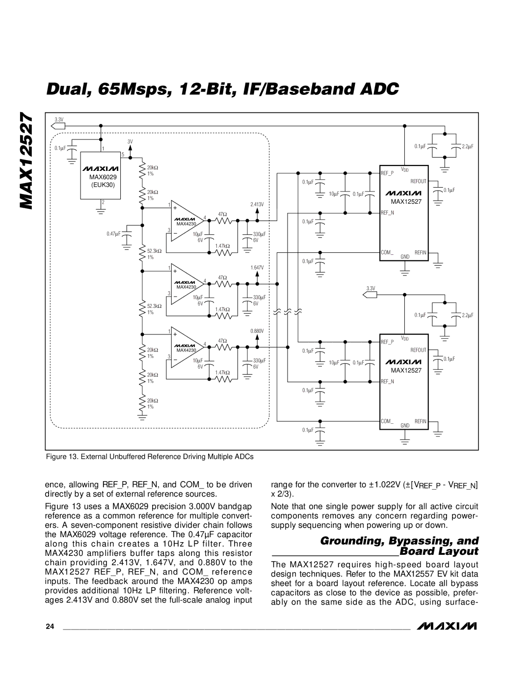
Figure 13. External Unbuffered Reference Driving Multiple ADCs
ence, allowing REF_P, REF_N, and COM_ to be driven directly by a set of external reference sources.
Figure 13 uses a MAX6029 precision 3.000V bandgap reference as a common reference for multiple convert- ers. A seven-component resistive divider chain follows the MAX6029 voltage reference. The 0.47µF capacitor along this chain creates a 10Hz LP filter. Three MAX4230 amplifiers buffer taps along this resistor chain providing 2.413V, 1.647V, and 0.880V to the MAX12527 REF_P, REF_N, and COM_ reference inputs. The feedback around the MAX4230 op amps provides additional 10Hz LP filtering. Reference volt- ages 2.413V and 0.880V set the full-scale analog input
range for the converter to ±1.022V (±[VREF_P - VREF_N] x 2/3).
Note that one single power supply for all active circuit components removes any concern regarding power- supply sequencing when powering up or down.
Grounding, Bypassing, and Board Layout
The MAX12527 requires
24 ______________________________________________________________________________________