Dual, 65Msps, 12-Bit, IF/Baseband ADC
MAX12527
Total Harmonic Distortion (THD)
THD is the ratio of the RMS sum of the first six harmon- ics of the input signal to the fundamental itself. This is expressed as:
| V 2 | + | V 2 | + | V 2 | + | V 2 | + | V 2 | + | V 2 | |
THD = 20 ⋅ log | 2 |
| 3 |
| 4 |
| 5 |
| 6 |
| 7 | |
|
|
|
|
|
|
|
|
|
|
| | |
|
|
|
|
|
| V1 |
|
|
|
|
| |
|
|
|
|
|
|
|
|
|
|
| |
where V1 is the fundamental amplitude, and V2 through V7 are the amplitudes of the 2nd- through
Spurious-Free Dynamic Range (SFDR)
SFDR is the ratio expressed in decibels of the RMS amplitude of the fundamental (maximum signal compo- nent) to the RMS value of the next largest spurious component, excluding DC offset.
Intermodulation Distortion (IMD)
IMD is the total power of the IM2 to IM5 intermodulation products to the Nyquist frequency relative to the total input power of the two input tones fIN1 and fIN2. The individual input tone levels are at
3 x fIN2 + fIN1, 2 x fIN1 - 2 x fIN2, 2 x fIN1 + 2 x fIN2, 2 x fIN2 - 2 x fIN1
3 x fIN1 - 2 x fIN2, 3 x fIN2 - 2 x fIN1, 3 x fIN1 + 2 x fIN2, 3 x fIN2 + 2 x fIN1, 4 x fIN1 - fIN2, 4 x fIN2 - fIN1,
4 x fIN1 + fIN2, 4 x fIN2 + fIN1
Note that the
3rd-Order Intermodulation (IM3)
IM3 is the total power of the
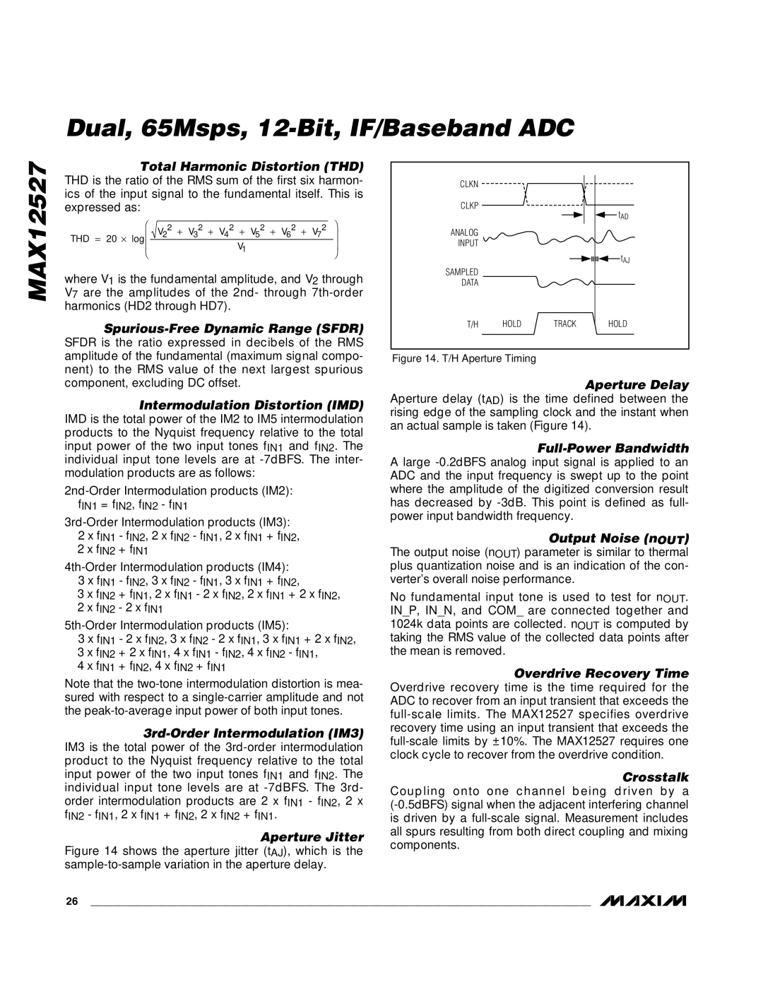
Aperture Jitter
Figure 14 shows the aperture jitter (tAJ), which is the sample-to-sample variation in the aperture delay.
CLKN
CLKP
tAD
ANALOG
INPUT
tAJ
SAMPLED
DATA
T/H | HOLD | TRACK | HOLD |
Figure 14. T/H Aperture Timing
Aperture Delay
Aperture delay (tAD) is the time defined between the rising edge of the sampling clock and the instant when an actual sample is taken (Figure 14).
Full-Power Bandwidth
A large
Output Noise (nOUT)
The output noise (nOUT) parameter is similar to thermal plus quantization noise and is an indication of the con- verter’s overall noise performance.
No fundamental input tone is used to test for nOUT. IN_P, IN_N, and COM_ are connected together and 1024k data points are collected. nOUT is computed by taking the RMS value of the collected data points after the mean is removed.
Overdrive Recovery Time
Overdrive recovery time is the time required for the ADC to recover from an input transient that exceeds the
Crosstalk
Coupling onto one channel being driven by a
26 ______________________________________________________________________________________