Dual, 65Msps, 12-Bit, IF/Baseband ADC
3.3V
0.1µF2.2µF
MAX12527
0.1µF1
5
MAX6029
(EUK21)
2
16.2kΩ
1µF
3
4
|
|
|
|
|
|
|
|
| 0.1µF | 2.048V |
5 |
|
|
|
|
|
|
| 300µF | ||
|
|
|
|
|
|
| 47Ω | |||
|
|
|
|
|
|
| ||||
|
|
|
|
| ||||||
|
|
| ||||||||
|
|
|
|
|
|
|
|
| ||
|
|
| 1 |
|
|
| 6V | |||
|
|
|
|
|
|
| ||||
|
|
|
|
|
| |||||
MAX4230
2
1.47kΩ
VDD
REFINREF_P
MAX12527
REF_N
REFOUTCOM_
0.1µF
10µF |
| 0.1µF |
|
0.1µF
0.1µF
GND
0.1µF
NOTE: ONE
3.3V
0.1µF2.2µF
0.1µF
VDD
REFINREF_P
MAX12527
REF_N
REFOUTCOM_
GND
0.1µF
10µF |
| 0.1µF |
|
0.1µF
0.1µF
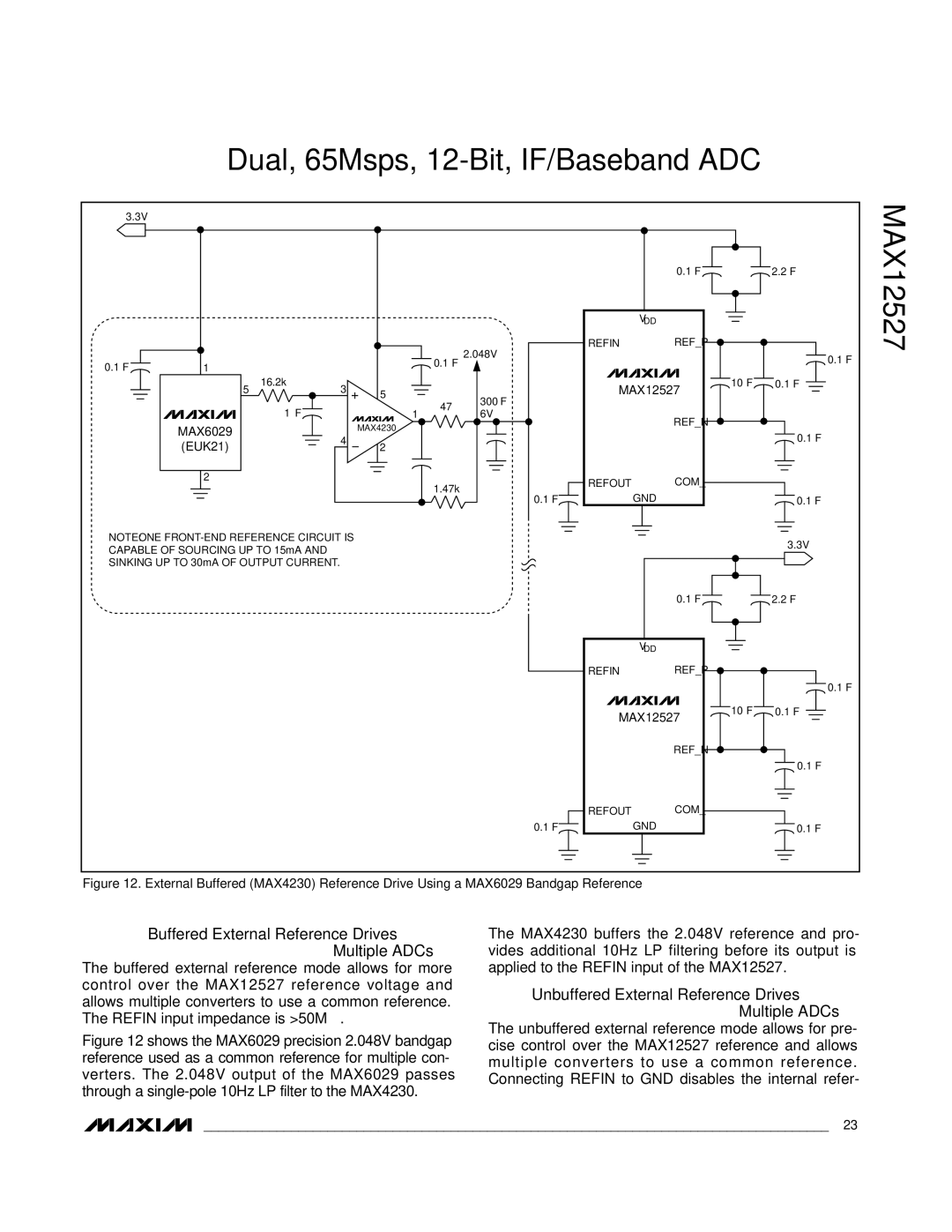
Figure 12. External Buffered (MAX4230) Reference Drive Using a MAX6029 Bandgap Reference
Buffered External Reference Drives Multiple ADCs
The buffered external reference mode allows for more control over the MAX12527 reference voltage and allows multiple converters to use a common reference. The REFIN input impedance is >50MΩ.
Figure 12 shows the MAX6029 precision 2.048V bandgap reference used as a common reference for multiple con- verters. The 2.048V output of the MAX6029 passes through a single-pole 10Hz LP filter to the MAX4230.
The MAX4230 buffers the 2.048V reference and pro- vides additional 10Hz LP filtering before its output is applied to the REFIN input of the MAX12527.
Unbuffered External Reference Drives Multiple ADCs
The unbuffered external reference mode allows for pre- cise control over the MAX12527 reference and allows multiple converters to use a common reference. Connecting REFIN to GND disables the internal refer-
______________________________________________________________________________________ 23