SSE
Page
UHF Range 2 450-488 MHz Portable Radio
SSE
For safe usage contained in the Product Safety and RF
Before using this product, read the operating instructions
Foreword
Exposure booklet enclosed with your radio
Table of Contents
Chapter Performance Checks
Chapter
Chapter Encryption
Chapter Radio Alignment Procedures
Chapter Troubleshooting Charts
Chapter Troubleshooting
Chapter Troubleshooting Tables
Chapter Troubleshooting Waveforms
Appendix B Replacement Parts Ordering
Appendix a Accessories
Related Publications
Glossary
Viii November 11
MHz Clock Waveform
List of Figures
List of Tables
Special Note on Nypd Warranty Agreement
Commercial Warranty
Limited Warranty
What This Warranty Covers And For How Long
What This Warranty Does Not Cover
IV. How To Get Warranty Service
II. General Provisions
III. State Law Rights
VII. Governing Law
VI. Patent And Software Provisions
Xiv
Physical Features of the Radio
Radio Description
FLASHport
Position
Portable Radio Model Numbering System
Item Number Description
SSE 5000 UHF Range 2 450-488 MHz Model Chart
General Receiver Transmitter
Specifications for UHF Range 2 450-488 MHz Radios
Injury
Notations Used in This Manual
Radio Description Notations Used in This Manual
Major Assemblies
Theory of Operation
Receiving
Mode of Operation
RX LNA
Transmitting
Part Number Description
Power Distribution
V5A
V3A V3D
DC Power Routing-VOCON Board
DC Power Routing-Transceiver Board
Output Description Name
V3A
Voltage Output Voltage
Supply Output Supply Type Unprogrammed Circuits Supplied
Vocon Connector P1
Battery Connector J3
Transceiver Board
Interconnections
Serial Eeprom
Antenna Ports
Receiver
Power Conditioning Components
Receiver Front-End
UHF Range
Receiver Back-End
Transmitter
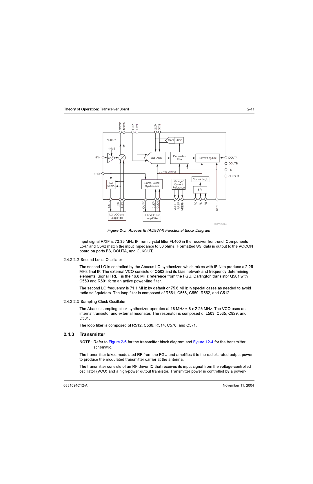
Abacus III AD9874 Functional Block Diagram
Power Distribution
Power Amplifier Transistor Q107
Driver Amplifier
Antenna Switch
Directional Coupler
Harmonic Filter
Power-Control IC Pcic U104
RF Detector D101
Pin Name Description
Vlim
VAR2
VAR1
VAR3
Frequency Generation Unit FGU
Reference Oscillator Y200
Fractional-N Frequency Synthesizer FracN IC U202
Vocon Board
Loop Filter
VCO Buffer IC Vcobic
Universal Flex Connector J102
Transceiver Board Connector P201
Functional Blocks
External Interface Module EIM
Microcontroller Unit MCU
Baseband Interface Port BBP
Digital Signal Processor DSP
System Clocks
General-Purpose Input/Output Gpio Module
Gcap II IC U501
Audio and Power
MCU Interface
Voltage Regulation
Audio Circuitry
Interface Support
Audio PA Status Mode Voltage
USB Transceiver
One-Wire Support
Watchdog Timer
KHz Oscillator and Cmos Output
MHz Reference Generation for Gcap II IC
Universal Side Connector
Universal Connector and Option Selects
Pin Number Description
Display Module
Controls and Control Top Flex
Function Option Select Voltage
Transmit Audio Path
Vocon Audio Paths
Gcap II IC U501
Receive Audio Path
Theory of Operation Vocon Board
Radio Power-Up/Power-Down Sequence
Test Equipment and Service Aids
Levels of Service
Test Equipment
2Test Equipment and Service Aids Test Equipment
Motorola
Service Aids
Part Description Application
Number
ChipMaster Options
Motorola Service Part Description Application
Service Level
Motorola Part Description Application Number
SOIC-14/SOL-16J
Field Programming
Performance Checks
Test Equipment Setup
Radio Test Mode
Access the Test Mode
System Analyzer Test Set Power Supply
ESN
Display Description Appears
Test Channel
RF Test Mode
No. Display Description Function Tones
Astro
Control Top Test Mode
Receiver Performance Checks
Test Mode CSQ
Test Name System Analyzer Radio Test Set Comments
Sinad
Transmitter Performance Checks
Performance Checks Transmitter Performance Checks
Radio Alignment Test Setup
Radio Alignment Procedures
Reading the Radio
Tuner Menu
Radio Information
Transmitter Alignments
Softpot
Reference Oscillator Alignment
Band Target
Transmit Power Alignment
Watts
Transmit Power
Transmit Power Alignment Screen High Power
Transmit Deviation Balance Alignment Screen
Transmit Deviation Balance Alignment
Transmit Deviation Limit Alignment Screen
Transmit Deviation Limit Alignment
Performance Testing
Battery Reading Calibration
Transmitter Test Pattern
11. Battery Reading Calibration Screen
Multikey Feature
Encryption
Load an Encryption Key
Encryption Multikey Feature
General Maintenance
Disassembly/Reassembly Procedures
Cleaning
Inspection
Handling Precautions
SSE 5000 Exploded View
SSE 5000 Exploded View
NNTN4825 KIT, Back Chassis includes items
NNTN4826 KIT, Front Chassis includes items
Battery
Disassembly/Reassembly Procedures for Accessories
Antenna
Attach the Antenna
Remove the Battery
Attach the Battery
Belt Clip
Attach the Belt Clip
Attaching the Belt Clip
Remove the Belt Clip
Assembling the Carry Case
Carry Case
Universal Connector Dust Cover
Disassembly/Reassembly Procedures for Radio Knobs
Remove the Universal Connector Dust Cover
Attach the Universal Connector Dust Cover
Volume Knob
Install the Channel Select Knob
Remove the Volume Knob
Channel Select Knob
Install the Volume Knob
Disassembly Procedures for SSE 5000 Radio
Separate the Chassis and Housing Assemblies
Disassemble the Chassis Assembly
Disassemble the Control Top
Disassemble the Housing Baseplate
Reassemble the Control Top
Reassembly Procedures for SSE 5000 Radio
Join the Chassis and Housing Assemblies
Reassemble the Chassis Assembly
Reassemble the Housing Baseplate
November 11
Voltage Measurement and Signal Tracing
Troubleshooting
Signal Name Nominal Value Tolerance Vocon Board Source
Standard Bias Table
Error Description Error Type Corrective Action Code
Power-Up Error Codes
Operational Error Codes
Receiver Troubleshooting
Error Code Description Corrective Action
Encryption Troubleshooting
Transmitter Troubleshooting
Symptom Possible Cause Corrective Action
PL, DPL, MDC
List of Troubleshooting Charts
Troubleshooting Charts
Vocon
Main Troubleshooting Flowchart
Power-Up Failure-Page
OK?
DC Supply Failure-Page
Host C
VHF U1
Display Failure-Page
Regsel
Check Active Low Status on both Reset and CS
Control top/PTT
Volume Set Error
RTA3 RTA2 RTA1 RTA0
Channel Select Error
PTT
Button Test
Top/Side Button Test
VCO TX/RX
VCO TX/RX Unlock
OK?
Vocon TX Audio-Page
TX RF
RX SAP
Vocon RX Audio-Page
Check Preamp Output Signal At C530
Rxlo
RX RF-Page
Vocon RX
LNA
RX RF-Page
UHF
TX RF-Page
Measure RF levels at C723
Temp
Vocon
Keyload Failure
Synopsis
Secure Hardware Failure
Troubleshooting Charts Secure Hardware Failure
List of Board and IC Signals
Troubleshooting Tables
J707 Description To/From Pin No
J102 Side Description Probe Point Connector Pin No Number
J701 Description
J701 Description To/From Pin No
ADV
Reset
Address
Ground Data
Enoe
VPP
CS1
CS2
Address Ground Not Used Data
Eepotinc
Hostwake Batteryid
Extspkrsel
Audiopaen
Boot
Encreset
KPROW2
KPROW3
URTS1XRXD
URXD1USBVMI
Adtrig
URXD2
Spimisoa Misoa
Not Used Btdisable
Spimisob Misob
Not Used Eepromsel
Unisel
Abacuscs
Flprcs
Gcapce
UTXD1USBVPO
UCTS1USBSPEED
Usbvmo
Usbtxen Khzint
Kvlusbdet
Onewireen
Not Used Batbusen
Usbvpi
CKO
EB1N
Oeen
Ebon
Wait
TXDOBDI5V
RXDINENC3V
RXDIN5V
RTS
Onewireopt
Flprcs Uartint Gcapresetx
Spimosib Mosib
Spimisob Misoa
TXDOBDIENC3V
RTSFILLSEN3V CTSFILLREQ3V
TXDOBDIUP3V
AD4BDID
XTAL1
Battery Auxbat Auxfet
XTAL2 PRSC2
LX2
Pasense PGM0
Padrv
LS3RX
Dgnd
AGND3
Simio AD5VOLUME
Dwnout Dwnin
Cmpout Dscinn
Micinneg
10-24
List of Waveforms
Troubleshooting Waveforms
MHz Clock Waveform
11.2 13 MHz Clock
Trace 1 Buffer input at R452 Trace 2 Buffer output at C452
11.3 16.8 MHz Buffer Input and Output
768 kHz Clock Outputs Waveforms
11.4 32.768 kHz Clock Outputs
SPI B Data Waveforms
SPI B Data
Receive Serial Audio Port SAP Waveforms
Receive Serial Audio Port SAP
Receive Baseband Interface Port RX BBP Waveforms
Receive Baseband Interface Port RX BBP
Transmit Baseband Interface Port TX BBP Waveforms
Transmit Baseband Interface Port TX BBP
List of Vocon Schematics, Board Layouts and Parts Lists
Schematics, Board Layouts, and Parts Lists
Txalc
Transceiver RF Board
NUE7337 Receiver Front-End Circuit
NUE7337 Receiver Back-End Circuit
NUE7337 Transmitter and Automatic Level Control Circuits
NUE7337 Frequency Generation Unit Synthesizer Circuit-1
NUE7337 Frequency Generation Unit Synthesizer Circuit-2
NUE7337 DC Power
NUE7337 Antenna Switch and Harmonic Filter
NUE7337 Transceiver RF Board Layout-Side
10. NUE7337 Transceiver RF Board Layout-Side
NUE7337 Transceiver RF Board Parts List
CAP Chip 7.0PF 16V .5PF
CAP Chip 8.0PF 16V .5PF
CAP Chip 12.0 PF 5% COG
CAP CER Chip 4.7UF
Battery
Connector Contact
Contact RF Connector
COIL, 6.8 UH Power
Notplaced 64AM Dummy Part Number PCB
MA,.58OHM,SM
HDI Layers
Tstr P-CH Hdtmos
IC VHF/UHF/800 MHZ Ldmos Driver
Module Direct Coupler
IC Temperture Sensor
IC PWR Ctrl in MOS20
Schematics, Board Layouts, and Parts Lists Vocon Board
12. NCN6186 Vocon Board Overall Circuit Schematic-Sheet 2
13. NCN6186 Vocon Universal Connector Circuit
14. NCN6186 Vocon Flipper Circuit
15. NCN6186 Vocon Controller and Memory Circuits-Sheet 1
16. NCN6186 Vocon Controller and Memory Circuits-Sheet 2
17. NCN6186 Vocon Audio and DC Circuits
18. NCN6186 Vocon DC Clocks
19. NCN6186 Vocon Display-RF Interface
20. NCN6186 Vocon Spark Gaps
21. NCN6186 Vocon Board Layout-Side
22. NCN6186 Vocon Board Layout-Side
NCN6186 Vocon Board Parts List
Coil 47UH SMT Power
Connector
IC Single FET BUS Switch
LED Stanley Bicolor RED
Ohms
IC Cmos Bilateral Switch
Power Management
IC Spdt Switch
Shield SUB Patriot
Control Flex
23. Control Flex Overall Circuit Schematic
24. Control Flex Board Layout-Side
Universal Flex
26. Universal Flex Overall Circuit Schematic
27. Universal Flex Board Layout-Side
12.5 UCM
29. UCM Flex Overall Circuit Schematic
30. UCM Board Layout-Side
Appendix a Accessories
Microphones and Microphone Accessories
Keyload Accessories
Surveillance Accessories
Programming Cables
Appendix B Replacement Parts Ordering
Product Customer Service
Fax Orders
Parts Identification
ALC
Glossary
Term Definition
Codeplug
Epot
KVL
MCU
OSW
Reset
Sram
Tsop
Glossary-10 November 11
Vocon
Index
Specifications
Index-3
Index-4
Page
Motorola, Inc West Sunrise Boulevard Ft. Lauderdale, FL
6881094C12-A