Manuals
/
Omega
/
Computer Equipment
/
Computer Hardware
Omega
OME-A822PG
manual
User’sGuide
Models:
OME-A822PG
1
1
63
63
Download
63 pages
60.32 Kb
1
2
3
4
5
6
7
8
Specs
Analog Input Signal Connection
Default base address is
Programmable Timer/Counter
Warranty
Hardware Configuration
Diagnostic Utility
Setup
Connector
Jumper Settings
Page 1
Image 1
User’sGuide
Shop online at
www.omega.com
e-mail:
info@omega.com
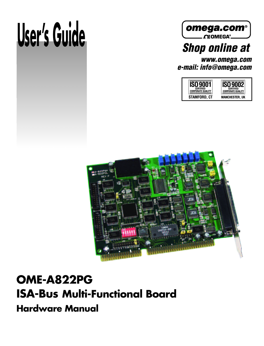
OME-A822PG
ISA-Bus
Multi-Functional
Board
Hardware Manual
Page 1
Page 2
Page 1
Image 1
Page 1
Page 2
Contents
User’sGuide
Mexico
Canada
Benelux
Czech Republic
OME-A-822PGH/PGL
Introduction
Tables of Contents
Connector
General Description
Features
Power Consumption
Specifications
Analog Inputs
3 A/D Converter
Digital I/O
DA Converter
Interrupt Channel
Direct Memory Access Channel DMA
Programmable Timer/Counter
Product Check List
Applications
Board Layout
Hardware Configuration
Default base address is
I/O Base Address Setting
1 JP1 D/A Internal Reference Voltage Selection
Jumper Settings
3 JP3 Single-ended/Differential Selection
2 JP2 D/A Int/Ext Ref Voltage Selection
5 JP5 Interrupt Level Selection
4 JP4 A/D Trigger Source Selection
6 JP6 User Timer/Counter Clock Input Selection
DRQ JP7 Dack JP8 DMA
7 JP7 DMA Dack Selection JP8 DMA DRQ Selection
Address Read Write
I/O Register Address
2 A/D Input Buffer Register
1 8254 Counter
Conversion is completed, the Ready bit will clear to zero
3 D/A Output Latch Register
Clear Interrupt Request
4 D/I Input Buffer Register
GAIN3 GAIN2 GAIN1 GAIN0
6 A/D Gain Control Register
7 A/D Multiplex Control Register
OME-A-822PGH Gain Control Code Table
8 A/D Mode Control Register
9 A/D Software Trigger Control Register
10 D/O Output Latch Register
CN2
Digital I/O
Counter
8254 Timer/Counter
A/D Conversion
Polling, interrupt and DMA
1 A/D conversion flow
3 A/D Transfer Modes
2 A/D Conversion Trigger Modes
Delay the settling time refer to Sec .4.6 and Sec
Using software trigger and polling transfer
Refer to Sec
D/A Conversion
Analog Input Signal Connection
OME-A-822PGL/PGH Hardware Manual
OME-A-822PGL/PGH Hardware Manual
Use a single connection to frame ground not A.GND or D.GND
Signal Shielding
Using OME-DB-8225 CJC Output
CN1 Digital Input Pin Assignment
CN1/CN2/CN3 Pin Assignment
CN2 Digital Output Pin Assignment
SINGLE-ENDED Signal Mode
Differential Signals
OME-DB-8225
Daughter Board
OME-DB-37
OME-DB-16P
Description of Variable Resistors
Calibration
D/A Calibration
A/D Calibration
Introduction
Diagnostic Utility
OME-A-822PGL/PGH Hardware Manual
Running The Diagnostic Utility
Base address selection screen
Setup
DMA no and IRQ no selection screen
Calibration
Function Test
Test Test Screen
Digital I/O Test Screen
Multiplexer Test Screen
Use IRQ Test Screen
Use DMA Test Screen
DA Gain Test Screen
Timer 0 Test Screen
Special Test
Help
WARRANTY/DISCLAIMER
Temperature
Top
Page
Image
Contents