KX-P7100
7 Component Reference Guide
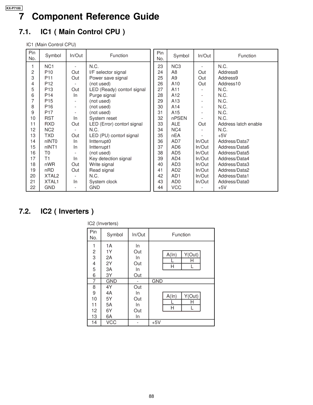
7.1.IC1 ( Main Control CPU )
IC1 (Main Control CPU)
Pin | Symbol | In/Out | Function | |
No. | ||||
|
|
| ||
1 | NC1 | - | N.C. | |
2 | P10 | Out | I/F selector signal | |
3 | P11 | Out | Power save signal | |
4 | P12 | - | (not used) | |
5 | P13 | Out | LED (Ready) contorl signal | |
6 | P14 | In | Purge signal | |
7 | P15 | - | (not used) | |
8 | P16 | - | (not used) | |
9 | P17 | - | (not used) | |
10 | RST | In | System reset | |
11 | RXD | Out | LED (Error) contorl signal | |
12 | NC2 | - | N.C. | |
13 | TXD | Out | LED (PU) contorl signal | |
14 | nINT0 | In | Intterrupt0 | |
15 | nINT1 | In | Intterrupt1 | |
16 | T0 | - | (not used) | |
17 | T1 | In | Key detection signal | |
18 | nWR | Out | Write signal | |
19 | nRD | Out | Read signal | |
20 | XTAL2 | - | N.C. | |
21 | XTAL1 | In | System clock | |
22 | GND | - | GND | |
|
|
|
|
Pin | Symbol | In/Out | Function | |
No. | ||||
|
|
| ||
23 | NC3 | - | N.C. | |
24 | A8 | Out | Address8 | |
25 | A9 | Out | Address9 | |
26 | A10 | Out | Address10 | |
27 | A11 | - | N.C. | |
28 | A12 | - | N.C. | |
29 | A13 | - | N.C. | |
30 | A14 | - | N.C. | |
31 | A15 | - | N.C. | |
32 | nPSEN | - | N.C. | |
33 | ALE | Out | Address latch enable | |
34 | NC4 | - | N.C. | |
35 | nEA | - | +5V | |
36 | AD7 | In/Out | Address/Data7 | |
37 | AD6 | In/Out | Address/Data6 | |
38 | AD5 | In/Out | Address/Data5 | |
39 | AD4 | In/Out | Address/Data4 | |
40 | AD3 | In/Out | Address/Data3 | |
41 | AD2 | In/Out | Address/Data2 | |
42 | AD1 | In/Out | Address/Data1 | |
43 | AD0 | In/Out | Address/Data0 | |
44 | VCC | - | +5V | |
|
|
|
|
7.2.IC2 ( Inverters )
IC2 (Inverters)
Pin | Symbol | In/Out |
| Function | ||
No. |
| |||||
|
|
|
|
|
| |
1 | 1A | In |
|
|
|
|
2 | 1Y | Out |
|
|
|
|
| A(In) | Y(Out) |
| |||
3 | 2A | In |
|
| ||
| L | H |
| |||
4 | 2Y | Out |
|
| ||
| H | L |
| |||
5 | 3A | In |
|
| ||
|
|
|
| |||
6 | 3Y | Out |
|
|
|
|
7 | GND | - | GND |
|
| |
8 | 4Y | Out |
|
|
|
|
9 | 4A | In |
|
|
|
|
| A(In) | Y(Out) |
| |||
10 | 5Y | Out |
|
| ||
| L | H |
| |||
11 | 5A | In |
|
| ||
| H | L |
| |||
12 | 6Y | Out |
|
| ||
|
|
|
| |||
13 | 6A | In |
|
|
|
|
14 | VCC | - | +5V |
|
| |
88