[2] Circuit description of control PWB
2) 27C020 (IC8):
EPROM of 2Mbit equipped with software for the main CPU.
1. General description
Fig. 2 shows the functional blocks of the control PWB, which is com- posed of 4 blocks.
MAIN | PANEL | MECHANISM/ | |
RECORDING | |||
CONTROL | CONTROL | ||
CONTROL | |||
BLOCK | BLOCK | ||
BLOCK | |||
|
|
MODEM
BLOCK
3) W24257S-70LL (IC7): pin-28 SOP (SRAM)
Line memory for the main CPU system RAM area and coding/decoding process. Used as the transmission buffer.
Memory of recorded data such as daily report and auto dials. When the power is turned off, this memory is backed up by the lithium battery.
4) KM29N040T (IC9):
A 512×8bit NAND FLASH MEMORY to store the voice and image data when using memory functions.
Fig. 2 Control PWB functional block diagram
2. Description of each block
(1) Main control block
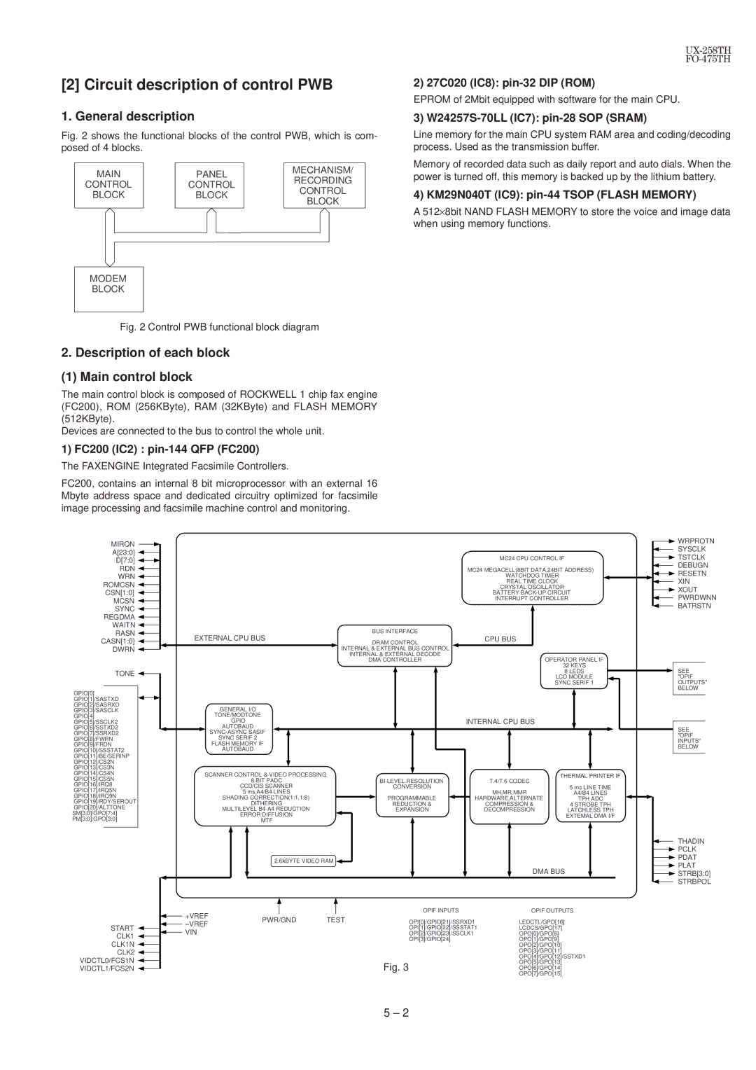
The main control block is composed of ROCKWELL 1 chip fax engine (FC200), ROM (256KByte), RAM (32KByte) and FLASH MEMORY (512KByte).
Devices are connected to the bus to control the whole unit.
1) FC200 (IC2) : pin-144 QFP (FC200)
The FAXENGINE Integrated Facsimile Controllers.
FC200, contains an internal 8 bit microprocessor with an external 16 Mbyte address space and dedicated circuitry optimized for facsimile image processing and facsimile machine control and monitoring.
MIRQN
A[23:0] ![]()
D[7:0] ![]()
![]()
RDN ![]()
WRN ![]()
ROMCSN ![]()
CSN[1:0] ![]()
MCSN ![]()
SYNC ![]()
REGDMA ![]()
WAITN ![]()
RASN ![]()
CASN[1:0] ![]()
DWRN 
TONE 
GPIO[0]
GPIO[1]/SASTXD GPIO[2]/SASRXD GPIO[3]/SASCLK
GPIO[4]
GPIO[5]/SSCLK2
GPIO[6]/SSTXD2
GPIO[7]/SSRXD2
GPIO[8]/FWRN
GPIO[9]/FRDN
GPIO[10]/SSSTAT2
GPIO[11]/BE/SERINP
GPIO[12]/CS2N
GPIO[13]/CS3N
GPIO[14]/CS4N
GPIO[15]/CS5N
GPIO[16]/IRQ8
GPIO[17]/IRQ5N
GPIO[18]/IRQ9N
GPIO[19]/RDY/SEROUT
GPIO[20]/ALTTONE
SM[3:0]/GPO[7:4]
PM[3:0]/GPO[3:0]
START
CLK1 ![]()
CLK1N ![]() CLK2
CLK2 ![]()
VIDCTL0/FCS1N 
VIDCTL1/FCS2N 
MC24 CPU CONTROL IF
MC24 MEGACELL(8BIT DATA,24BIT ADDRESS)
| WATCHDOG TIMER |
| REAL TIME CLOCK |
| CRYSTAL OSCILLATOR |
| BATTERY |
| INTERRUPT CONTROLLER |
BUS INTERFACE |
|
EXTERNAL CPU BUS | CPU BUS |
DRAM CONTROL |
|
INTERNAL & EXTERNAL BUS CONTROL |
|
INTERNAL & EXTERNAL DECODE | OPERATOR PANEL IF |
DMA CONTROLLER | |
| 32 KEYS |
| 8 LEDS |
| LCD MODULE |
| SYNC SERIF 1 |
GENERAL I/O
TONE/MODTONE
GPIOINTERNAL CPU BUS
AUTOBAUD
SYNC SERIF 2
FLASH MEMORY IF
AUTOBAUD
SCANNER CONTROL & VIDEO PROCESSING |
|
| THERMAL PRINTER IF | |||
|
|
| T.4/T.6 CODEC |
| ||
| CCD/CIS SCANNER |
| CONVERSION |
|
| 5 ms LINE TIME |
| 5 ms,A4/B4 LINES |
|
|
| MH,MR,MMR | A4/B4 LINES |
| SHADING CORRECTION(1:1,1:8) |
| PROGRAMMABLE | HARDWARE,ALTERNATE | TPH ADC | |
| DITHERING |
| REDUCTION & |
| COMPRESSION & | 4 STROBE TPH |
| MULTILEVEL |
| EXPANSION |
| DECOMPRESSION | LATCHLESS TPH |
| ERROR DIFFUSION |
|
|
|
| EXTEMAL DMA I/F |
| MTF |
|
|
|
|
|
| 2.6kBYTE VIDEO RAM |
|
|
|
| |
|
|
|
|
| DMA BUS |
|
+VREF |
|
| OPIF INPUTS |
| OPIF OUTPUTS | |
PWR/GND | TEST | OPI[0]/GPIO[21]/SSRXD1 |
| LEDCTL/GPO[16] |
| |
|
|
| ||||
VIN |
|
| OPI[1]/GPIO[22]/SSSTAT1 | LCDCS/GPO[17] |
| |
|
| OPI[2]/GPIO[23]/SSCLK1 |
| OPO[0]/GPO[8] |
| |
|
|
| OPI[3]/GPIO[24] |
| OPO[1]/GPO[9] |
|
|
|
|
|
| OPO[2]/GPO[10] |
|
|
|
|
|
| OPO[3]/GPO[11] |
|
|
|
|
|
| OPO[4]/GPO[12]/SSTXD1 | |
|
|
| Fig. 3 |
| OPO[5]/GPO[13] |
|
|
|
|
| OPO[6]/GPO[14] |
| |
OPO[7]/GPO[15]
![]() WRPROTN
WRPROTN
SYSCLK
![]() TSTCLK
TSTCLK
DEBUGN
![]()
![]() RESETN
RESETN
XIN
![]() XOUT
XOUT
PWRDWNN BATRSTN
SEE "OPIF
OUTPUTS" BELOW
SEE "OPIF
INPUTS" BELOW
THADIN
![]() PCLK
PCLK
![]() PDAT
PDAT
![]() PLAT
PLAT
![]() STRB[3:0]
STRB[3:0]
STRBPOL
5 – 2
