TMS320C6202

FIXED-POINT DIGITAL SIGNAL PROCESSOR

SPRS072B ± AUGUST 1998 ± REVISED AUGUST 1999

SYNCHRONOUS-BURST MEMORY TIMING

timing requirements for synchronous-burst SRAM cycles (see Figure 15)

NO.


'C6202-200

'C6202-233

'C6202-250

UNIT


MIN MAX

MIN MAX

MIN

MAX


7

tsu(EDV-CKO2H)

Setup time, read EDx valid before CLKOUT2

2.5

2.1

2


ns

high


8

th(CKO2H-EDV)Hold time, read EDx valid after CLKOUT2 high

1.5

1.5

1.5


ns

switching characteristics for synchronous-burst SRAM cycles²³ (see Figure 15 and Figure 16)

NO.


PARAMETER

'C6202-200

'C6202-233

'C6202-250

UNIT


MIN

MAX

MIN

MAX

MIN

MAX


Output setup time,


valid


1

tosu(CEV-CKO2H)


CEx

2P ± 5.5


2P ± 4.4


2P ± 3.8


ns


before CLKOUT2 high


Output hold time,


valid after


2

toh(CKO2H-CEV)


CEx

1


1


1


ns

INFORMATION


CLKOUT2 high


3

tosu(BEV-CKO2H)


Output setup time,

BEx

valid

2P ± 5.5


2P ± 4.4


2P ± 3.8


ns


before CLKOUT2 high


Output hold time,


invalid


4

toh(CKO2H-BEIV)


BEx

1


1


1


ns


after CLKOUT2 high


5

tosu(EAV-CKO2H)


Output setup time, EAx valid

2P ± 5.5


2P ± 4.4


2P ± 3.8


ns


before CLKOUT2 high


6

toh(CKO2H-EAIV)


Output hold time, EAx invalid

1


1


1


ns


after CLKOUT2 high


Output setup time,


9

tosu(ADSV-CKO2H)


SDCAS/SSADS valid before

2P ± 5.5


2P ± 4.4


2P ± 3.8


ns

ADVANCE


CLKOUT2 high


Output hold time,


10

toh(CKO2H-ADSV)


SDCAS/SSADS valid after

1


1


1


ns


CLKOUT2 high


Output setup time,


11

tosu(OEV-CKO2H)


SDRAS/SSOE valid before

2P ± 5.5


2P ± 4.4


2P ± 3.8


ns


CLKOUT2 high


Output hold time,


12

toh(CKO2H-OEV)


SDRAS/SSOE

1


1


1


ns


valid after CLKOUT2 high


13

tosu(EDV-CKO2H)


Output setup time, EDx valid

2P ± 5.5


2P ± 4.4


2P ± 3.8


ns


before CLKOUT2 high§


14

toh(CKO2H-EDIV)


Output hold time, EDx invalid

1


1


1


ns


after CLKOUT2 high


Output setup time,


15

tosu(WEV-CKO2H)


SDWE/SSWE

2P ± 5.5


2P ± 4.4


2P ± 3.8


ns


valid before CLKOUT2 high


Output hold time,


16

toh(CKO2H-WEV)


SDWE/SSWE

1


1


1


ns


valid after CLKOUT2 high


²P = 1/CPU clock frequency in ns. For example, when running parts at 250 MHz, use P = 4 ns.

³ SDCAS/SSADS, SDRAS/SSOE, and SDWE/SSWE operate as SSADS, SSOE, and SSWE, respectively, during SBSRAM accesses.

§For the first write in a series of one or more consecutive adjacent writes, the write data is generated one CLKOUT2 cycle early to accommodate the ED enable time.

POST OFFICE BOX 1443 HOUSTON, TEXAS 77251±1443

35

Page 35
Image 35
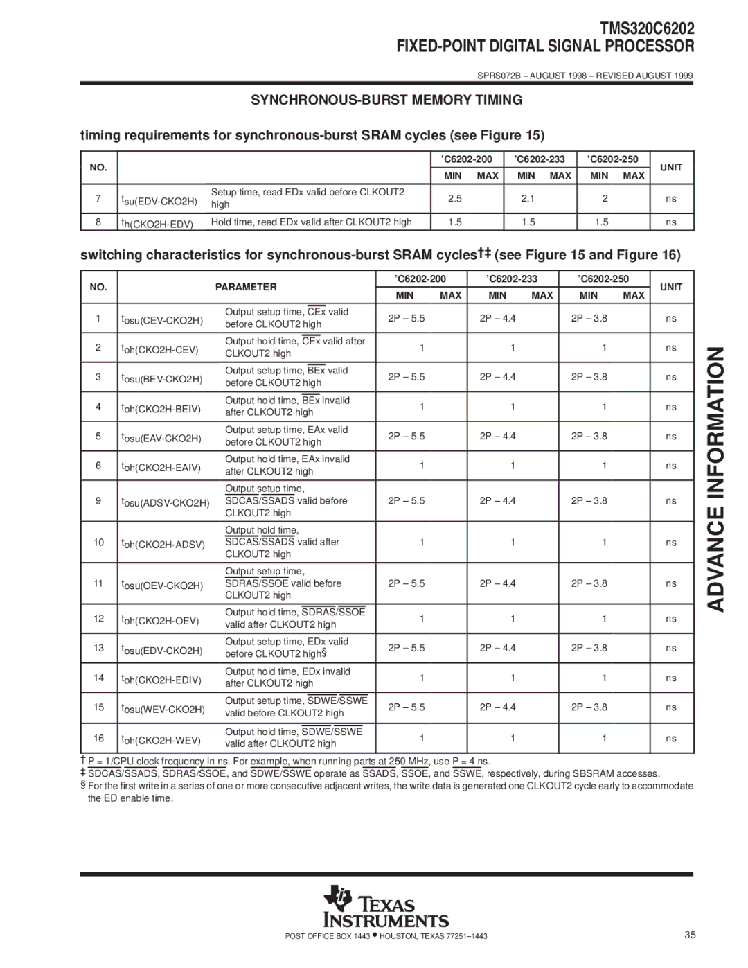
Texas Instruments TMS320C6202 specifications SYNCHRONOUS-BURST Memory Timing, Unit MIN MAX

TMS320C6202 specifications

The Texas Instruments TMS320C6202 is a powerful digital signal processor (DSP) that is well-regarded in the realm of high-performance computing applications. As part of the TMS320C6000 family, the C6202 was designed to meet the demanding requirements of telecommunications, audio and video processing, and other real-time digital signal processing tasks.

One of the primary features of the TMS320C6202 is its superscalar architecture. This allows the processor to execute multiple instructions simultaneously, significantly improving throughput and efficiency. With two functional units, the DSP can execute both fixed-point and floating-point operations in parallel, optimizing performance for various computational workloads.

The core clock frequency of the TMS320C6202 typically reaches up to 150 MHz, which means it can process instructions at impressive speeds. This high frequency, combined with an advanced instruction set that includes efficient looping and branching instructions, makes the C6202 highly adept at handling complex algorithms common in digital signal processing.

Memory access is another critical characteristic of the TMS320C6202. It supports a unified memory architecture featuring both on-chip SRAM and external memory interfaces. This enables seamless data transfer between the processor and memory, improving overall system performance. The processor can interface with diverse memory types, including SDRAM and other high-speed memory technologies, further enhancing its versatility.

Furthermore, the TMS320C6202 incorporates a range of built-in features designed to facilitate efficient development. Its integrated hardware multipliers and accumulators allow rapid computation of mathematical functions, while on-chip debugging support simplifies the development process. Additionally, the processor features a host of peripheral interfaces, enabling integrations for input/output operations, essential for real-time applications such as multimedia processing.

Texas Instruments excels in providing software and development tools for the TMS320C6202. The Code Composer Studio (CCS) and various libraries enhance the ease of programming and optimization for this DSP, which helps engineers accelerate product development.

Overall, the Texas Instruments TMS320C6202 is a robust digital signal processor characterized by its high-speed performance, dual functional units, innovative memory architecture, and support for sophisticated algorithms. It has become a preferred choice for applications requiring intensive signal processing capabilities, making significant contributions to fields such as telecommunications, multimedia, and industrial automation.