ADSP-2186
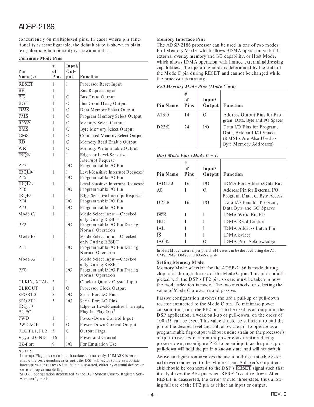
concurrently on multiplexed pins. In cases where pin func- tionality is reconfigurable, the default state is shown in plain text; alternate functionality is shown in italics.
Common-Mode Pins
|
| # | Input/ |
|
Pin | of | Out- |
| |
Name(s) | Pins | put | Function | |
RESET | 1 | I | Processor Reset Input | |
BR | 1 | I | Bus Request Input | |
BG | 1 | O | Bus Grant Output | |
BGH | 1 | O | Bus Grant Hung Output | |
DMS | 1 | O | Data Memory Select Output | |
PMS | 1 | O | Program Memory Select Output | |
IOMS | 1 | O | Memory Select Output | |
BMS | 1 | O | Byte Memory Select Output | |
CMS | 1 | O | Combined Memory Select Output | |
RD | 1 | O | Memory Read Enable Output | |
WR | 1 | O | Memory Write Enable Output | |
IRQ2/ | 1 | I | Edge- or | |
|
|
|
| Interrupt Request1 |
PF7 |
| I/O | Programmable I/O Pin | |
IRQL0/ | 1 | I | ||
PF5 |
| I/O | Programmable I/O Pin | |
IRQL1/ | 1 | I | ||
PF6 |
| I/O | Programmable I/O Pin | |
IRQE/ | 1 | I | ||
PF4 |
| I/O | Programmable I/O Pin | |
PF3 | 1 | I/O | Programmable I/O Pin | |
Mode C/ | 1 | I | Mode Select | |
|
|
|
| only During RESET |
PF2 |
| I/O | Programmable I/O Pin During | |
|
|
|
| Normal Operation |
Mode B/ | 1 | I | Mode Select | |
|
|
|
| only During RESET |
PF1 |
| I/O | Programmable I/O Pin During | |
|
|
|
| Normal Operation |
Mode A/ | 1 | I | Mode Select | |
|
|
|
| only During RESET |
PF0 |
| I/O | Programmable I/O Pin During | |
|
|
|
| Normal Operation |
CLKIN, XTAL | 2 | I | Clock or Quartz Crystal Input | |
CLKOUT | 1 | O | Processor Clock Output | |
SPORT0 | 5 | I/O | Serial Port I/O Pins | |
SPORT1 | 5 | I/O | Serial Port I/O Pins | |
IRQ1:0 |
|
|
| Edge- or |
FI, FO |
|
| Flag In, Flag Out2 | |
PWD | 1 | I | ||
PWDACK | 1 | O | ||
FL0, FL1, FL2 | 3 | O | Output Flags | |
VDD and GND | 16 | I | Power and Ground | |
9 | I/O | For Emulation Use | ||
|
|
|
|
|
NOTES
1Interrupt/Flag pins retain both functions concurrently. If IMASK is set to enable the corresponding interrupts, the DSP will vector to the appropriate interrupt vector address when the pin is asserted, either by external devices or set as a programmable flag.
2SPORT configuration determined by the DSP System Control Register. Soft- ware configurable.
Memory Interface Pins
The
Full Memory Mode Pins (Mode C = 0)
| # |
|
|
| of | Input/ |
|
Pin Name | Pins | Output | Function |
|
|
|
|
A13:0 | 14 | O | Address Output Pins for Pro- |
|
|
| gram, Data, Byte and I/O Spaces |
D23:0 | 24 | I/O | Data I/O Pins for Program, |
|
|
| Data, Byte and I/O Spaces |
|
|
| (8 MSBs Are Also Used as |
|
|
| Byte Memory Addresses) |
|
|
|
|
Host Mode Pins (Mode C = 1) |
| ||
|
|
|
|
| # |
|
|
| of | Input/ |
|
Pin Name | Pins | Output | Function |
|
|
|
|
IAD15:0 | 16 | I/O | IDMA Port Address/Data Bus |
A0 | 1 | O | Address Pin for External I/O, |
|
|
| Program, Data, or Byte Access |
D23:8 | 16 | I/O | Data I/O Pins for Program, |
|
|
| Data Byte and I/O Spaces |
IWR | 1 | I | IDMA Write Enable |
IRD | 1 | I | IDMA Read Enable |
IAL | 1 | I | IDMA Address Latch Pin |
IS | 1 | I | IDMA Select |
IACK | 1 | O | IDMA Port Acknowledge |
|
|
|
|
In Host Mode, external peripheral addresses can be decoded using the A0, CMS, PMS, DMS, and IOMS signals.
Setting Memory Mode
Memory Mode selection for the
Passive configuration involves the use a
Active configuration involves the use of a
nal driver connected to the Mode C pin. A driver’s output en- able should be connected to the DSP’s RESET signal such that it only drives the PF2 pin when RESET is active (low). After
RESET is deasserted, the driver should
REV. 0 |
